ARM’s Mali Midgard Architecture Explored
by Ryan Smith on July 3, 2014 11:00 AM ESTMidgard’s Arithmetic Pipelines
Having taken a look at Midgard’s architecture from a high level perspective, we next want to dive deep into the heart of Midgard: its arithmetic pipelines. This is where the bulk of the work takes place on any modern GPU, and in most cases real-world GPU performance significantly hinges on the design decisions made here. Furthermore this is where Midgard’s most unconventional design decisions lie, and as a result it’s the arithmetic pipelines that make Midgard stand apart from anything else we’ve seen.
ARM describes Midgard as a Very Long Instruction Word (VLIW) design with Single Instruction Multiple Data (SIMD) characteristics (though officially it is called Sequential Long Instruction Word). What this means is that at a high level ARM is feeding multiple ALUs, including SIMD units, with a single long word of instructions. But perhaps it’s better we start at a low level instead.
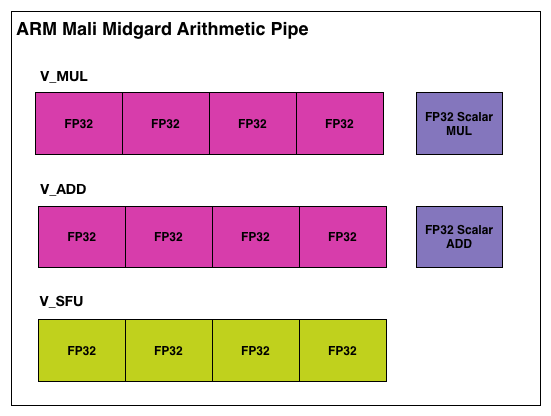
The above is a single Midgard arithmetic pipeline, in our example configured for FP32 operations. In it ARM uses a mix of both scalar and vector (SIMD) ALUs. Altogether ARM breaks it down as 3 vector ALUs and 2 scalar ALUs, each responsible for a specific type of operation.
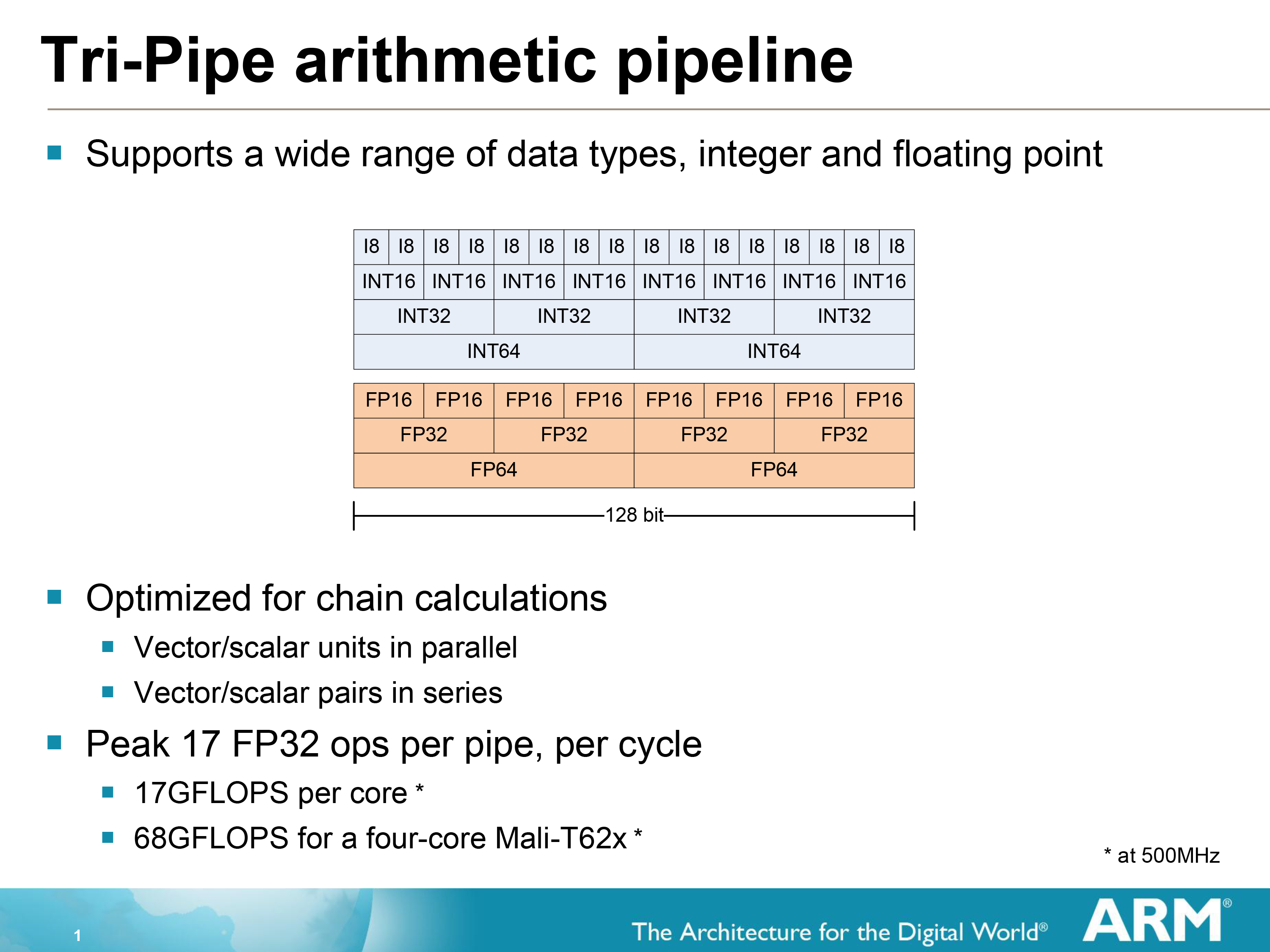
If we stop for a moment and look at the SIMD, we find out something very interesting about it as well. Remember earlier how we mentioned that Midgard is capable of 64bit operations? Well this is how they do it. Not with separate 64bit and 32bit units as in some other designs, but by using a single 128bit wide SIMD and decomposing operations based on their width. The 128bit SIMDs in a Midgard core can process 2 64 bit operations, 4 32bit operations, or even 8 16bit operations per clock cycle. Simply fill the SIMD with as many (identical) operations as will fit, and the SIMD will handle the rest.
The use of SIMDs and SIMD-like designs is not uncommon in GPUs, but it’s relatively rare to see a flexible SIMD of this nature. In the past other architecture designers have talked about this being a efficiency tradeoff – you lose some efficiency by using a flexible design rather than a rigid design – however in ARM’s case they have decided that they can meet all of their goals with a 128bit SIMD.
Jumping back up a level, from a hardware perspective a Midgard arithmetic pipeline is capable of up to 17 FP32 FLOPS. This is constructed as the following.
- 4 vector adds
- 4 vector multiplies
- 1 scalar add
- 1 scalar multiple
- 1 FDOT4 dot product (7 FLOPS)
The vector and scalar operations are relatively self-explanatory, while the dot products are a result of using the vector special functions unit. To that end every architecture possesses SFUs in some form to handle dot products, transcendentals, and other complex operations, but their inclusion in FLOPS counting is uncommon. Most architectures merely count FLOPS as adds and multiplies through the ubiquitous and all important MAD (Multiply-Add) instruction. NVIDIA’s forthcoming K1 (to pick a GPU with a desktop counterpart) has 192 FP32 ALUs, and via MADs can achieve up to 384 FLOPS per cycle.
Ultimately how ARM counts FLOPS is entirely up to them, but we do want to take a moment to rectify it with how we count FLOPS on our end. Dot products are a relatively common mathematical operation in rendering, enough so that it’s important to be able to do them quickly, but they are generally not counted for computing FLOPS.
Meanwhile for FP64 FLOPS, as one would expect Midgard’s performance is much lower. ARM does not provide the FLOPS breakdown for 64bit operations, but they tell us that it is a total of 5 FLOPS. Our best guess here is that 4 of those FLOPS are coming from the vector units (2 FP64 MADs) and then 1 more FP64 FLOP is coming off of the scalar units, which if our assumption is correct would imply that it is not capable of an FP64 MAD in 1 cycle. Overall on a MAD basis this puts FP64 performance at 5/10ths, or ½ FP32 performance, which is a very high FP64 performance ratio even compared to desktop GPU architectures.
Furthermore, in further rectifying how ARM presents some of its data with how we typically present data in our articles, we’re also going to be using a condensed version of the Midgard arithmetic pipeline from this point on. As most architectures either utilize ALUs that can perform a MAD on their own or simplify their descriptions to showcase 1 ALU (rather than explicitly over 2 ALUs as on Midgard), we will be using a condensed version of the Midgard arithmetic pipeline that is drawn in a similar manner. Since we always count a standard ALU as being capable of 2 FLOPs (SFUs withstanding), this makes our Midgard arithmetic pipeline illustration consistent with our previous illustrations. It’s for all intents and purposes the same pipeline, only condensed.
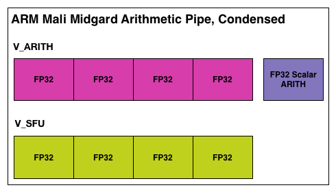
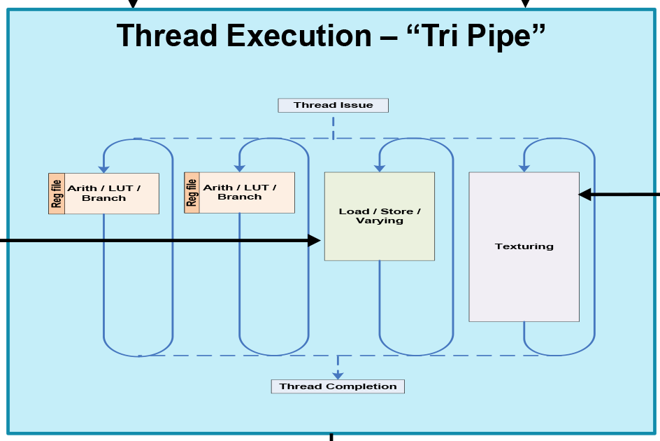
Finally, let’s take a quick look at a complete Midgard “tri pipe” core from an ALU standpoint. Since in T760 each core has 2 arithmetic units, a single core a just 2 of our condensed units. For a complete GPU this would then be multiplied by as many cores as the resulting design called for.


66 Comments
View All Comments
tuxRoller - Monday, July 7, 2014 - link
Yup, that is indeed what I said earlier.I don't think anand is interested in investigating that avenue, however. For one, he might fear that such published info would blacklist him from future qualcomm info dumps (pretty far fetched, imho, but AT likes the corporate relationships its been able to cultivate). For another, AT doesn't seem to be terribly interested in oss.
prabindh - Monday, July 7, 2014 - link
Do the GFLOPS give a measure of how much performance an OpenCL kernel can provide in ARM Mali architecture ? Simple fp16/32 kernels doing a MAD and writing to global memory do not seem to match the GFLOPS calculated here. Are there other HW LD/ST limits in the pipeline (assuming no system memory Bandwidth limitations) ?Amadiro - Friday, July 11, 2014 - link
So how do the dFdx/dFdy operators work for such a non-wavefront based design? Does using them imply a huge overhead/stall/context-switch of some sort on this kind of architecture?MrSpadge - Wednesday, August 13, 2014 - link
Thanks ARM, Ryan and Anandtech for this very interesting article! This finally gives this "yet another SoC GPU irrelevant to me" a face. And I think ARM could employ this design for some very nice GP-GPU (co-)processors:- FP64 performance rivaling the best
- not relying on TLP could open up the GPU for entire new application ranges where they just didn't make sense yet
- ARM can scale the amount of compute per core easily
I know building a massive GP-GPU chip is anything but trivial.. but this seems an architecture worthy of this!
manoj1919 - Friday, September 25, 2015 - link
Hi Anand,Nice article!.I am working with mali GPU, and I am a researcher trying to figure out power management capabilities of MALI GPU. last part of this article seems to be covering a bit of that. can you please point me to the source of ARM's slide showing gating techniques of MALI GPU(last figure in article).
Thanks in advance,
Manoj
gregware - Monday, February 20, 2017 - link
Interesting article, thanks!