ARM’s Mali Midgard Architecture Explored
by Ryan Smith on July 3, 2014 11:00 AM ESTTricks of the Trade: Transaction Elimination and Frame Buffer Compression
While we have spent some time covering various techniques ARM uses to improve efficiency in Midgard, we wanted to spend a bit more time talking about two specific techniques in general that we find especially cool: transaction elimination and frame buffer compression.
Going back once again to what we said earlier about rendering and power efficiency, any rendering work ARM can eliminate before it’s completed not only improves performance by freeing up resources, but it also frees up power by not having to spend it on said redundant work. This is especially the case for anything that wants to hit system memory, as compared to the on-die caches and memories available to the GPU, system memory is slow and expensive to operate from a power perspective.
For their final two tricks then, having already eliminated as much rendering work as possible through other means, ARM’s last tricks involve minimizing the amount of data from rendered tiles and pixels that needs to hit system memory. The first of these tricks is Transaction Elimination (TE), which is based on the idea that if a scene (or parts of it) do not change, then it makes no sense to spend power and bandwidth rewriting those identical screen portions.
![]()
To accomplish this, ARM relies on their tiling system to break down the scene for them, and from there they can begin comparing tiles that are waiting for finalization (ROP/blending) to the tiles that are already in the frame buffer from the previous frame. Using a simple cyclic redundancy check to compare the tiles, if the tile to be rendered is found to be identical to the tile already there, the tile can be skipped and the memory bandwidth saved. Altogether of all of ARM’s various tricks, this is among the simplest conceptually.
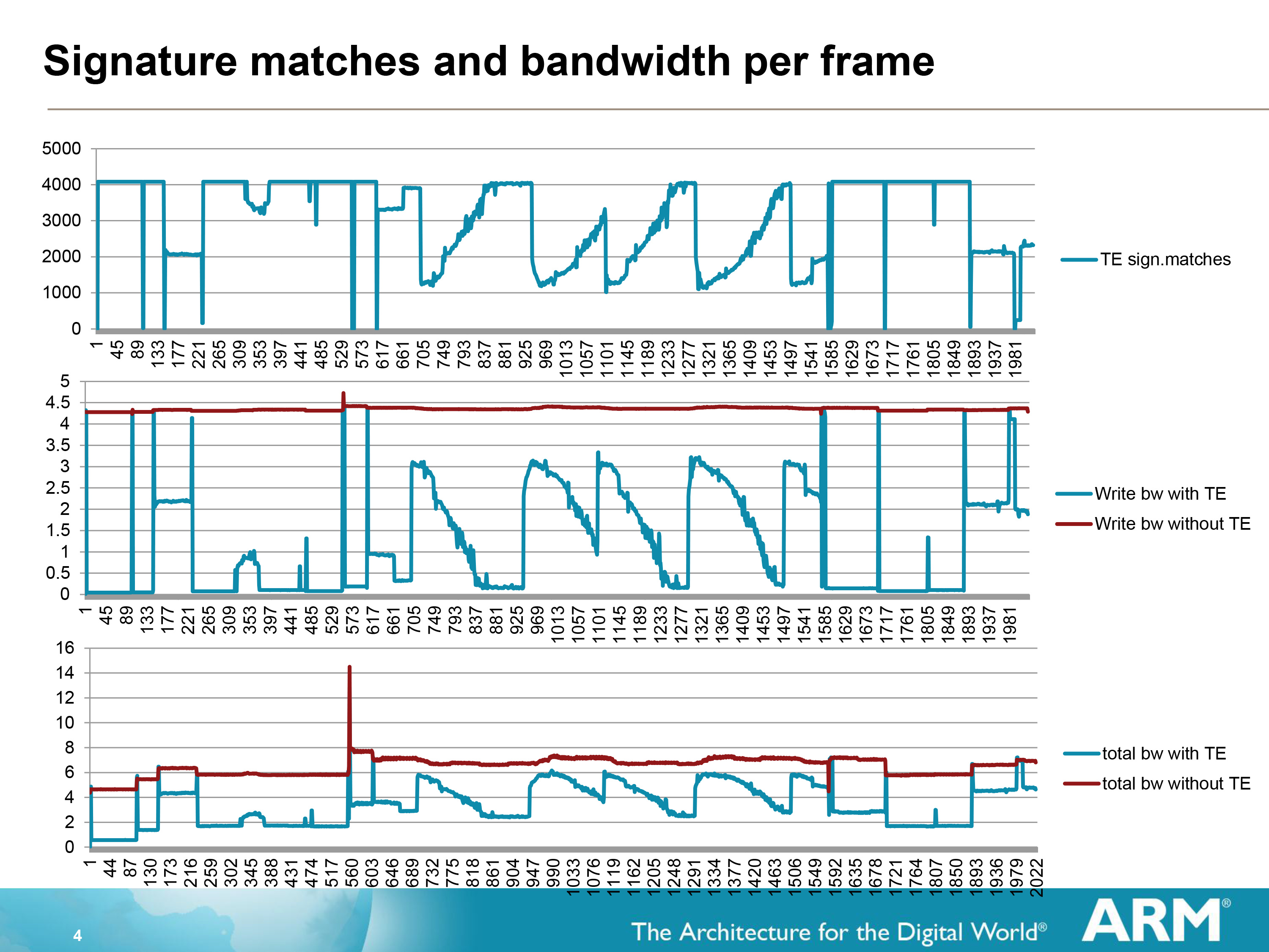
The effectiveness of Transaction Elimination in turn depends on the content. A generally static workload such as a movie will have a high degree of redundancy overall (notably when the camera is not moving), while a game may have many moving elements but will still have redundant elements that can be skipped. As a result ARM can save anywhere between almost nothing and over 99% for a highly static workload, with the average more than offsetting the roughly 1.5% overhead from computing and comparing the CRCs.
Of course Transaction Elimination does have one drawback besides its low overhead, and that is CRC collisions. During a CRC collision a pair of tiles that are different will compute to the same CRC value, and as such Transaction Elimination will consider them identical and throw away the new tile. With a standard CRC value being 64bits, such a collision is rare but not impossible, and indeed will statistically occur sooner or later. In which case Transaction Elimination has no fallback method; it is judge, jury, and executioner as it were, and the new tile will be lost.
As a result Transaction Elimination is interestingly imprecise in a world of precision. When a collision occurs the displayed tile will be wrong, but only for as long as there is a collision, which in turn should only be for 1 frame, or 1/60th of a second.
Moving on, when worse comes to worse and ARM does need to write a new tile, on the Mali-T700 series GPUs they can turn to ARM Frame Buffer Compression (AFBC) to minimize the amount of memory bandwidth they spend on that operation. By using a lossless compression algorithm to write out and store a frame, memory bandwidth is saved on both the writing of the frame and in the reading of it.
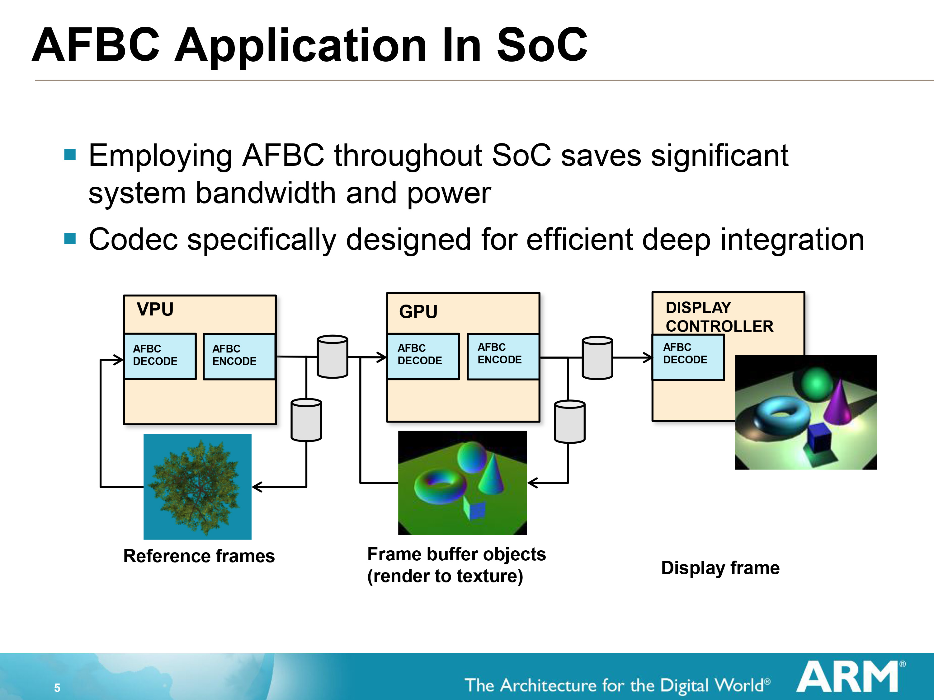
AFBC requires that both the GPU and the Display Controller support the technology, as the frame remains compressed the entire time until decompressed for display/consumption. Interestingly this means that the GPU needs to be able to compress as well as decompress, as it can reuse its own frames either in frame buffer objects (where a frame is rendered to a texture) or in Transaction Elimination. This becomes a secondary vector of saving bandwidth since it results in similar bandwidth savings for the frame even if the frame is never touched by the display controller itself. A similar principle applies to ARM’s video decoders (VPUs) which can use AFBC to compress a frame before shipping it off to the GPU.
On that note, it’s worth pointing out that while AFBC is an ARM technology, for interoperability purposes ARM does license it out to other display controller designers. ARM puts together their own display controllers, but because SoC integrators can use one of many display controllers it’s to ARM’s own benefit that everyone else be able to read AFBC as well as ARM can.


66 Comments
View All Comments
seanlumly - Thursday, July 3, 2014 - link
Given the "exotic" the ILP and the 128-bit VLIW SIMD, the Mali looks like an impressive performer. If a Mali T760MP10 is indeed a part fit for smartphone-level power consumption, then a quick linear-scaling -- given GFXBench scores of a T760MP4 -- would imply that such a GPU is very competitive with something like the adreno 420 and certainly impressive if scaled up further to a tablet-level power consumption. If, however, an MP10 consumes roughly as much as a K1 or GX6650, then I'm very sceptical about its competitive performance.I find the distribution of ALUs to memory units strange given mobile bandwidth limits. The Mali T760 in an 8-core configuration clocked at 600MHz will allow for 19.2 GB/s of load/store access (256-bits/clock: source ARM). This is quite high memory bandwidth, and an increase in GPU clocks or cores will likely yield idling load/stores units doing nothing but taking up valuable die area. Operations with high varying access, cache reads, and tile read/writes will of course make good use of these additional units, but it still seems like overkill on all but very memory-access heavy apps. ARM would know best, though I'm suspicious that so many load/store units are needed for common workloads. I would guess that in common scenarios, bandwidth to main memory would be exhausted long before all of the memory units were fully utilized on a Mali T760 of high core count (eg. MP12-16).
Decoupling the load/stores and texture units as their own "core" may allow more appropriate scaling to fit the bandwidth of the target system. A system with an ultra-high resolution, could be endowed with more load/stores and/or texture units. A system with a lower resolution could use less and opt for more ALUs in the same space. This would be similar to big.LITTLE (different cores for different targeted workloads). In this scenario, the memory unit cores could be scaled independently of the ALU cores, perfectly tailored to the target system.
EdvardS - Friday, July 4, 2014 - link
Remember that there is a cache system between those units and the SoC memory controller. Bandwidth to the cores is quite different from bandwidth to the DDR memory.seanlumly - Friday, July 4, 2014 - link
Indeed! Bandwidth to cache, tile memory, varying data, or textures would likely be more relevant with a tile-based renderer that often exploits spatial locality when processing batches of pixels. This is especially true with modern screen-space effects that do multiple dependent reads per display pixel (eg. SSAO), but are strongly confined to buffer fragments surrounding the target pixel. Such situations would value having many LS/Tex units at little penalty.But I do still like the idea of an independently scalable "memory" core (containing load/store/texure pipes) to complement a "math" core (containing ALUs). A high-performance system targeting a 720p display will likely consume far less bandwidth than one targeting a 4K display, and as such, it would be nice to trade LS/Tex units for more ALUs in such a case.
Such an arrangement may also enable ARM more leeway when making predictions about a new architecture -- no doubt the Midgard arch was in development many years before it saw implementation in a retail product, which means that ARM would have had to guess trends (eg. resolution) far in advance to attain the right balance of on-chip units per core; independently scalable memory-cores would be more forgiving if the trends turned out not match the initial predictions.
seanlumly - Friday, July 4, 2014 - link
Actually, I am starting to understand the motivation behind the ratio of ALUs to Memory units in a Midgard core. I notice in GFXBench 3.0 "Manhattan", that the Mali T760MP4 (Rockchip rk3288) performs incredibly well at 720p, but it's performance drops off more than proportionately as the resolution increases. This may imply that in these higher than 720p scenarios, the 4-core variant of GPU may not be able to keep up with the memory demands, as computation should scale very close to proportionally.Thus the 1080p offscreen score for the Mail T760 MP4 in the GFXBench 3.0 (offline) database may be misleading as the MP4 may be a bit small for this resolution, and thus the performance may be low relative to its competition. A T760 MP8 would likely more than double the performance for a doubling of the resolution, pushing something like the Mali T760 MP8 well beyond the competition, at what I suspect are similar levels of power and die-size. I predict that a T760 MP8 would get slightly north of 16fps in GFXBench 3.0 (assuming adequate bandwidth to DDR). Even an MP6 variant of the GPU (as was the case with the T628 MP6 in the Exynos 5420) should put it more-or-less on-par with the competition!
The Mali performs even better in the GFXBench 2.7 "T-Rex" test, where a small 4-core Mali T760 MP4 surpasses the competition at 720p and even sub-720p resolutions in some instances! This is incredible. In this case, it seems that the test is more computation bound, as there is a more proportional scaling between performance and resolution.
I hope that future GPUs consider using the T760 in higher-core-count configurations. I still like the idea of a Memory-core, though I have little doubt that a Mali GPU of evenly matched size can go toe-to-toe with the competition.
Frenetic Pony - Friday, July 4, 2014 - link
Every time I read an overview of a SoC GPU I am so, so glad I don't do anything with mobile stuff. "We support tessellation! I mean, don't actually do it. Ever. But you know, it's supported."kkb - Friday, July 4, 2014 - link
How come there is no comparison with intel GPUs like the ones in Baytrail?darkich - Friday, July 4, 2014 - link
Because there is no comparison phrase.That GPU is completely inferior compared to latest Mali, PowerVR and Adreno architectures
Krysto - Friday, July 4, 2014 - link
Word.kkb - Monday, July 7, 2014 - link
well.. I don't really agree. Please look at the AT review from last week or so.. http://www.anandtech.com/show/8197/samsung-galaxy-...MEMO pad is a baytrail product and definitely performs better than MALI devices.
darkich - Monday, July 7, 2014 - link
Get your facts and reading skills in order.Firstly, the GPU in Memo Pad is definitely not definitely performing better than even the Mali T628, in fact those very tests show it trades blows with it, mostly due to much lower resolution screen.
Secondly, do you realize that the T760 is MUCH faster than T628?
You can see here that it is basically comparable to the Tegra K1 and even the intimidating Series 6XT doesn't trounce it.
Rest assured that any of these three, as well as the Adreno 420, is way above the ULP HD graphics chip