ARM’s Mali Midgard Architecture Explored
by Ryan Smith on July 3, 2014 11:00 AM ESTMidgard’s Arithmetic Pipelines
Having taken a look at Midgard’s architecture from a high level perspective, we next want to dive deep into the heart of Midgard: its arithmetic pipelines. This is where the bulk of the work takes place on any modern GPU, and in most cases real-world GPU performance significantly hinges on the design decisions made here. Furthermore this is where Midgard’s most unconventional design decisions lie, and as a result it’s the arithmetic pipelines that make Midgard stand apart from anything else we’ve seen.
ARM describes Midgard as a Very Long Instruction Word (VLIW) design with Single Instruction Multiple Data (SIMD) characteristics (though officially it is called Sequential Long Instruction Word). What this means is that at a high level ARM is feeding multiple ALUs, including SIMD units, with a single long word of instructions. But perhaps it’s better we start at a low level instead.
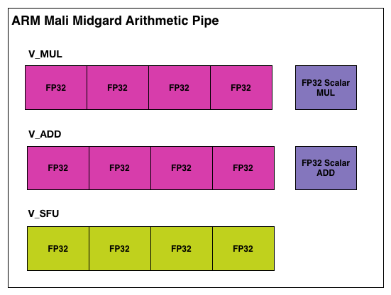
The above is a single Midgard arithmetic pipeline, in our example configured for FP32 operations. In it ARM uses a mix of both scalar and vector (SIMD) ALUs. Altogether ARM breaks it down as 3 vector ALUs and 2 scalar ALUs, each responsible for a specific type of operation.
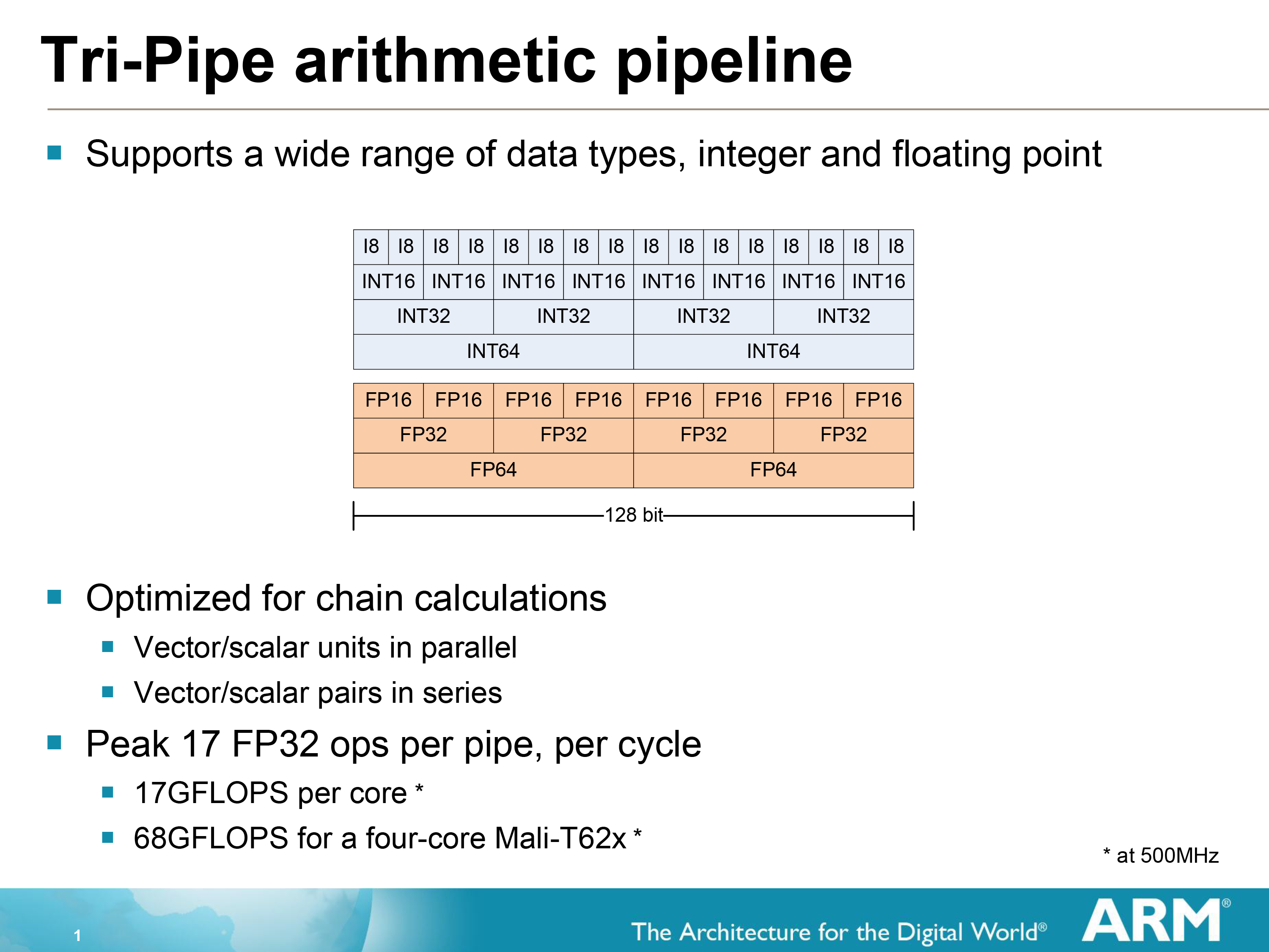
If we stop for a moment and look at the SIMD, we find out something very interesting about it as well. Remember earlier how we mentioned that Midgard is capable of 64bit operations? Well this is how they do it. Not with separate 64bit and 32bit units as in some other designs, but by using a single 128bit wide SIMD and decomposing operations based on their width. The 128bit SIMDs in a Midgard core can process 2 64 bit operations, 4 32bit operations, or even 8 16bit operations per clock cycle. Simply fill the SIMD with as many (identical) operations as will fit, and the SIMD will handle the rest.
The use of SIMDs and SIMD-like designs is not uncommon in GPUs, but it’s relatively rare to see a flexible SIMD of this nature. In the past other architecture designers have talked about this being a efficiency tradeoff – you lose some efficiency by using a flexible design rather than a rigid design – however in ARM’s case they have decided that they can meet all of their goals with a 128bit SIMD.
Jumping back up a level, from a hardware perspective a Midgard arithmetic pipeline is capable of up to 17 FP32 FLOPS. This is constructed as the following.
- 4 vector adds
- 4 vector multiplies
- 1 scalar add
- 1 scalar multiple
- 1 FDOT4 dot product (7 FLOPS)
The vector and scalar operations are relatively self-explanatory, while the dot products are a result of using the vector special functions unit. To that end every architecture possesses SFUs in some form to handle dot products, transcendentals, and other complex operations, but their inclusion in FLOPS counting is uncommon. Most architectures merely count FLOPS as adds and multiplies through the ubiquitous and all important MAD (Multiply-Add) instruction. NVIDIA’s forthcoming K1 (to pick a GPU with a desktop counterpart) has 192 FP32 ALUs, and via MADs can achieve up to 384 FLOPS per cycle.
Ultimately how ARM counts FLOPS is entirely up to them, but we do want to take a moment to rectify it with how we count FLOPS on our end. Dot products are a relatively common mathematical operation in rendering, enough so that it’s important to be able to do them quickly, but they are generally not counted for computing FLOPS.
Meanwhile for FP64 FLOPS, as one would expect Midgard’s performance is much lower. ARM does not provide the FLOPS breakdown for 64bit operations, but they tell us that it is a total of 5 FLOPS. Our best guess here is that 4 of those FLOPS are coming from the vector units (2 FP64 MADs) and then 1 more FP64 FLOP is coming off of the scalar units, which if our assumption is correct would imply that it is not capable of an FP64 MAD in 1 cycle. Overall on a MAD basis this puts FP64 performance at 5/10ths, or ½ FP32 performance, which is a very high FP64 performance ratio even compared to desktop GPU architectures.
Furthermore, in further rectifying how ARM presents some of its data with how we typically present data in our articles, we’re also going to be using a condensed version of the Midgard arithmetic pipeline from this point on. As most architectures either utilize ALUs that can perform a MAD on their own or simplify their descriptions to showcase 1 ALU (rather than explicitly over 2 ALUs as on Midgard), we will be using a condensed version of the Midgard arithmetic pipeline that is drawn in a similar manner. Since we always count a standard ALU as being capable of 2 FLOPs (SFUs withstanding), this makes our Midgard arithmetic pipeline illustration consistent with our previous illustrations. It’s for all intents and purposes the same pipeline, only condensed.
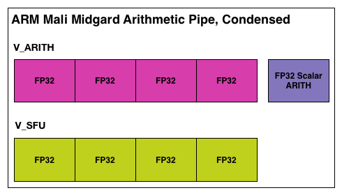
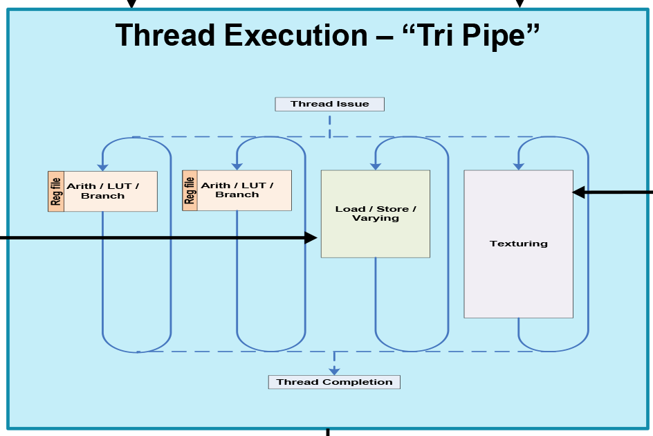
Finally, let’s take a quick look at a complete Midgard “tri pipe” core from an ALU standpoint. Since in T760 each core has 2 arithmetic units, a single core a just 2 of our condensed units. For a complete GPU this would then be multiplied by as many cores as the resulting design called for.


66 Comments
View All Comments
darkich - Friday, July 4, 2014 - link
You guys are missing the fact that Snapdragon 805 can reach a much higher memory bandwidth than Tegra K1.TheJian - Saturday, July 5, 2014 - link
But it still loses to K1 in most gpu stuff (all?). You're forgetting AMD/NV have had 20yrs of trying to figure out how to get the most they can from bandwidth for gaming. The devs have had that long working with their hardware also (game devs I mean). Everyone else has to play catch up here for years as they've never had to do anything game wise until last year or so as android etc gaming pumped up a bit.That is why you see ZERO Qcom optimized games (or did I miss one?) :) It's easier to optimize for a chip you already know inside out (amd/nv). I even went to Qcom's gaming page just to see if there were any games they had on their list that were REQUIRING snapdragon to see xx effects etc. There were none last I checked. All the games are just on googleplay with no snapdragon mention (like on NV games they say THD, and these games look quite a bit better than the regular versions) as they appear to work on ALL players chips. Google seems to be realizing K1 is where you want to be on gpu's at least for gaming centric stuff/automotive and I'd expect devs to continue to favor NV for optimizations as they don't need to learn a thing about k1 it's KEPLER which they've already spent 2yrs+ playing with (probably longer as they get dev versions long before we get a retail card so games can be made/optimized for them by the time they hit).
At 20nm xbox360/ps3 will be left behind as new games keep getting made on mobile. If you're not on xbox1/ps4 you'll be buying some cheap 20nm console box that has cheap games ($2-20 vs. $60 for xbox1/ps4) and as good or better graphics than last gen xbox360/ps3. GDC 2013 & 2014 surveys show devs are already massively making games for mobile and as 20nm kicks in everyone has K1 power levels or more. These android consoles/tv's etc will have more tricks than those ancient consoles so you should be able to get much better gaming experience on them for $100-200. The games pricing alone is a draw for poor people. With the ports happening right an left now of quality PC/console games and super cheap pricing there is even more reason to run to mobile for poor people who never played them before (half-life2, trine2, Serious Sam3BFE, none sold more than 11mil or so). There are a billion android users and most clearly have played none of this stuff even the console ports like Final Fantasy games, GTA games etc (on or off PC also doesn't matter) haven't been played by more than 10mil or so combined each. Lost of great stuff for poor people to pick up for under $10 in ports until the REAL new games for mobile hit this xmas/next xmas. All of the stuff the dev surveys show they've been working on will hit this year or next, and they are not angry birds games.
przemo_li - Tuesday, July 8, 2014 - link
Alternative view on Google stance:Nvidia is just first vendor that allowed them to show more features than are possible on Apples A7.
(Mobile-only vendors are not interested in full OpenGL...)
TheJian - Sunday, July 6, 2014 - link
If they're worried about lawsuits (odd they'd say that without merit), they must have had their lawyers tell them they'd be sued due to stealing tech that is probably from AMD/NV. DMCA takedowns, completely closing the kimono so to speak shows they are afraid for good reason. It isn't just competitor crap as nobody else is afraid of that it seems. The same tricks are being used by almost everyone to a large degree. So it seems to me they clearly owe someone some money and don't want to pay. They will probably show their details once they remove that stuff from a future gen soc or never I guess if they just can't remove it for some reason :)mczak - Thursday, July 3, 2014 - link
You could add Intel HD graphics (baytrail) though. Also quite interesting architecture-wise imho.btw some small correction wavefront size for amd (gcn) is 64, not 16 (I think this was wrong on older anandtech articles too). The simd size is 16 indeed but the same instruction is executed for 4 clocks always (on 16 different elements of the wavefront each clock).
mczak - Thursday, July 3, 2014 - link
Here's actually an explanation how the wavefront size of 64 works for gcn:http://devgurus.amd.com/thread/168154
Achtung_BG - Thursday, July 3, 2014 - link
My first touch phone is black LG Viewty in 2008 with Mali GPU :) :) :) If you have new article for android extention pack comparison with full Open GL will be very intrasting.Jedibeeftrix - Thursday, July 3, 2014 - link
yes please.i'd like to know:
1. how long until the AEP is rolled back into what will be OpenGL ES 4.0
1.1. whether it represents a subset of an existing OpenGL full-fat version (eg 4.4)
2. how this compares to DX 11.2 feature wise
2.1. whether AEP will be expanded in OpenGL ES 4.0 to make it broadly DX 11.2 compliant
przemo_li - Tuesday, July 8, 2014 - link
1) Never. (Though, separate extensions, can get into ES. AEP is just thin bundle over many other extensions)1.1) Yes. OpenGL 4.x is still capable of running AEP code.
2) DX11.2 is single vendor en-devour currently... (And You really should compare to F(eature)L(evel)11_2).
2.1) WHY?
Why on earth You need all those things?
Industry move in different direction. (Mantle, DX12, Metal, AZDO)
Doing stuff efficiently is new mantra now.
Adding more stuff from DX FL11_2 (Yes if You talk about features You MUST use F(eature)L(evels)!!!), would only complicate things for OpenGL ES.
We need AZDO.
Kevin G - Thursday, July 3, 2014 - link
I can see Qualcomm's concerns about a shader arms race in mobile: it has already happened on the CPU side without much benefit to the consumer. However, with the explosion in screen resolution in tablets, a spec race here would have a more tangible benefit for consumers. It sitll boggles my mind that a retina iPad has 50% more pixels and a slower GPU than my desktop system with a 1080p monitor driven by a GTX 770. My sole concern would be temperatures and power consumption.Well if Qualcomm isn't going to disclose the information, how much can be implied from driver information? Qualcomm purchased the mobile Radeon drivision from AMD back in 2009 and then came up with the anagram Adreno. If they're still using a design based upon what they got form AMD, it'd be reflective in similar drivers. If they've come up with a new architecture, it too would be evident in radically different drivers. The details would be lacking of course but some generalities could be made.