Samsung SSD 850 Pro (128GB, 256GB & 1TB) Review: Enter the 3D Era
by Kristian Vättö on July 1, 2014 10:00 AM ESTWhy We Need 3D NAND
For years, it has been known that traditional NAND (i.e. 2D NAND) is running on its last legs. Many analysts predicted that we would not see NAND scaling below 20nm because the reliability would simply be too low to make such a small lithography feasible. However, thanks to some clever engineering on both hardware and firmware sides NAND has scaled to 15nm without any significant issues but now the limit has been reached for real. To understand the limits of 2D NAND scaling, let's say hello to our old good friend Mr. N-channel MOSFET.

Unfortunately the diagram above is a bit too simplified to truly show what we need, so let's look at a real cross-section photo instead:
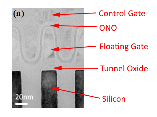
Let me walk you through the structure first. At the top is the control gate, which is a part of a structure known as a wordline. In a standard NAND design the control gate wraps around the floating gate and the two gates are separated by an insulating oxide-nitride-oxide layer (i.e. ONO), which is sometimes called Inter Poly Dielectric (IPD). Under the floating gate is the tunnel oxide, which is also an insulator, followed by the silicon substrate that acts as the bitline.
The reason why the control gate is wrapped around the floating gate is to maximize capacitance between the two. As you will soon learn, the capacitance between the gates is the key factor in NAND as it means that the control gate can control the floating gate.
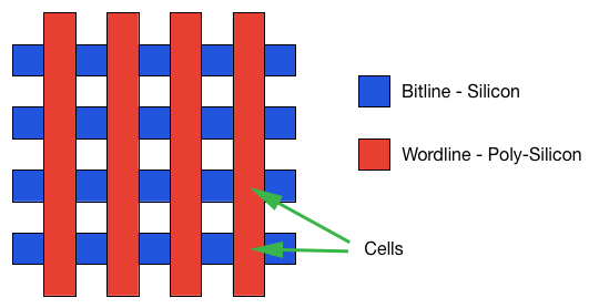
The purpose of bitlines and wordlines can be rather difficult to understand when looking at a cross-section, so here is what it all looks like from the top. Basically, bitlines and wordlines are just lines going in perpendicular directions and the floating gate and other materials reside between them.
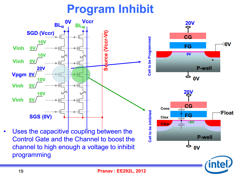
When programming a cell, a high voltage of around 20V is applied to the wordline of that cell. Of course, the problem is that you cannot apply voltage to just one cell because the whole wordline will be activated so in order to select a specific cell, the bitline of that cell is held at 0V. At the same time, the neighbouring bitlines are charged to about 6V because this increases the capacitance between the bitline and floating gate, which is turn negates enough of the capacitance between the control and floating gate that the electrons cannot tunnel through the tunnel oxide. This is crucial because if all the bitlines were held at 0V, then all the cells along that wordline would be programmed with the same value.
To erase a cell, a reverse operation is performed by keeping the wordline at 0V while issuing a ~20V voltage on the bitline, which makes the electrons flow in the opposite direction (i.e. from the floating gate back to the bitline/silicon).
The way NAND is programmed and erased is also its Achilles' Heel. Because such high voltage is needed, the insulators around the floating gate (i.e. ONO and tunnel oxide) wear out as the NAND goes through program and erase cycles. The wear out causes the insulators to lose their insulating characters, meaning that electrons may now be able to escape the floating or get trapped in tunnel oxide during a program or erase. This causes a change in the voltage state of the cell.
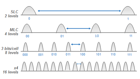
Remember, NAND uses the voltage states to define the bit value. If the charge in the floating gate is not what it is supposed to be, the cell may return an invalid value when read. With MLC and TLC this is even worse because the voltage states are much closer to each other, meaning that even minor changes in the voltage state may cause the voltage state to shift from its original position, which means the cell value will also change. Basically, MLC and TLC have less room for voltage state changes, which is why their endurance is lower because a cell that cannot hold its charge reliably is useless.
Now that we have covered the operation of NAND briefly, let's see what this has to do with scaling. Here is the same cross-section as above but with some dimensions attached.
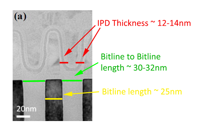
That is what a cross-section of a single cell looks like. When NAND is scaled, all these dimensions get smaller, which means that individual cells are smaller as well as the distance between each cell. The cross-section above is of IMFT's 25nm NAND (hence the bitline length of 25nm), so it is not exactly current generation but unfortunately I do not have any newer photos. There is no general rule to how much the dimensions shrink because 16nm simply means that one of the lengths is 16nm while others may not shrink that much.
The scaling introduces a variety of issues but I will start with the cell size. As the cell size is shrunk, the size of the floating gate is also shrunk, which means that the floating gate is able to hold less and less electrons every time the process node gets smaller. To put this into perspective, Toshiba's and SanDisk's 15nm NAND is stores less than 20 electrons per NAND cell. With TLC, that is less than three electrons per voltage state, so there is certainly not much headroom for escaped electrons. In other words, the cell becomes more vulnerable to the IPD and tunnel oxide wear out because even the loss of one electron can be vital to the voltage state.
The second issue is the proximity of the cells. The key factor in NAND is the capacitance between the control and floating gate but as the cells move closer to each other through scaling, the neighboring cells will also introduce capacitive coupling. In simpler terms, the neighboring cells will interfere more as the distance between the cells shrinks. The obstacle is that the interference varies depending on the charge of the neighbouring cell, so there is no easy way to exclude the intereference. This in turn makes programming harder and more time consuming because a higher voltage will be needed to achieve the sufficient capacitance between the control and floating gate to make the eletrons tunnel through the oxide.
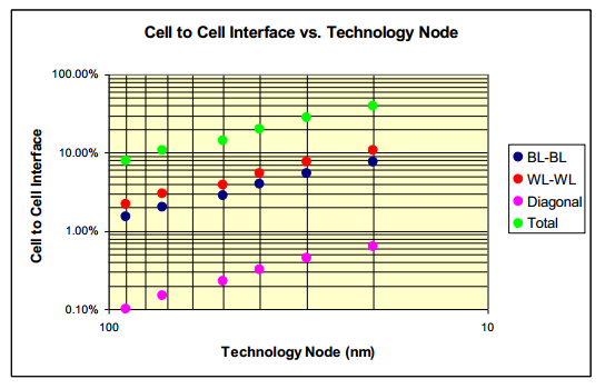
The graph above outlines historic rate of how cell to cell intereference increases through die shrinks. At 90nm, the interference was only around 8-9% but at 20nm it is a rather significant 40%. The interference means that 40% of the capacitive coupling comes from the other cells, making it very hard to control the gate you are trying to program or read. Fortunately as a result of some clever engineering (i.e. an airgap between the wordlines), the intererence is only about 25% at 25nm, which is much more managable than the 40% the historic rate would have given us.
The above can be fairly tough to digest, so let's do a simple analogy that everyone should be able to understand. Imagine that you have a bunch of speakers with each playing a different song. When these speakers are relatively large and far away from each other, it is easy to properly hear the song that the speaker closest to you is playing. Now, what happens if you bring the other speakers closer to the speaker you are listening? The other speakers will interfere and it becomes harder to tell your song apart from the others. If you turn down the volume or switch to smaller speakers with lower output volume, it becomes even harder to distinquish your song from the songs that the other songs that other speakers are playing. If you repeat this enough times, there will be a point when you are hearing your song as unclearly as the other songs.
The effect is essentially the same with NAND scaling. When the cells, or speakers in the analogy, move closer to each other, the amount of interference increases, making it harder to sense the cell or listen to the speaker. At the same time the size of the cell (or speakers) is shrunk, which further complicates the focus on one cell (or speaker).
That is NAND scaling and its issues in a nutshell. We have seen innovations such as airgaps between the wordlines to reduce cell-to-cell interference and a high K metal gate instead of a traditional ONO IPD to increase control gate to floating gate capacitance, but the limit has now been reached. However, like other semiconductors NAND must follow the Moore's Law in order to get more cost efficient. If you can no longer scale in the X and Y dimensions, what do you do? You hit the reset button and introduce the Z dimension.


160 Comments
View All Comments
YazX_ - Monday, July 7, 2014 - link
Prices are not going down, good thing we have Crucial who have best bang for the buck, ofcourse performance wise is not compared to sandisk or samsung, but its still a very fast SSD, for normal users and gamers, Mx100 is the best drive you can get for its price.soldier4343 - Thursday, July 17, 2014 - link
My next upgrade the Pro 850 512gb version over my OCZ 4 256gb.bj_murphy - Friday, July 18, 2014 - link
Thanks Kristian for such an amazing, in depth review. I especially loved the detailed explanation of current 2D NAND vs 3D NAND, how it all works, and why it's all so important. Possibly one of my favourite Anandtech articles to date!DPOverLord - Wednesday, July 23, 2014 - link
Looking at this it does not seem to be a HUGE difference than raid 0 of 2 Samsung Pro 840 512GB (1tb in raid 0).To upgrade at this point does not make the most sense.
Nickolai - Wednesday, July 23, 2014 - link
How are you implementing over-provisioning?joochung - Tuesday, July 29, 2014 - link
I don't see this mentioned anywhere, but were the tests performed with RAPID enabled or disabled? I understand that some of the tests could not run with RAPID enabled, but for those other tests which do run on a formatted partition (i.e. not run on the raw disk), its not clear if RAPID is enabled or disabled. Therefore its not clear how RAPID will affect the results in each test.Rekonn - Wednesday, July 30, 2014 - link
Anyone know if you can use the 850 Pro ssds on a Dell PERC H700 raid controller? Per documentation, controller only supports 3 Gb/s SATA.janos666 - Thursday, August 14, 2014 - link
I always wondered if there is any practical and notable difference between dynamic and static over-provisioning.I mean... since TRIM should blank out the empty LBAs anyway, I don't see the point in leaving unpartitioned space for static over-provisioning for home users. From a general user standpoint, having as much usable space available as possible (even if we try to restrict ourself from ever utilizing it all) seems to be a lot more practical (until it's actually usable with an acceptable speed, so even if notably slower but still fast enough...) than keeping a (significantly more, but still not perfectly) constant random write performance.
So, I always create a system partition as big as possibly (I do the partitioning manually: a minimal size EFI boot partition + everything else at one piece) without leaving unpartitioned space for over-provisioning and I try to leave as much space empty as possible.
However, one time, after I filled my 840 Pro up to ~95% and I kept it like that for 1-2 days, it never "recovered" . Even after I manually ran "defrag c: /O" to make sure the freed up space is TRIMed, sequential write speeds were really slow and random write speeds were awful. I ha to create a backup image with DD, fill the drive with zeros a few times and finally run an ATA Secure Erase before restoring the backup image.
Even though I was never gentle with the drive (I don't do stupid things like disabling swapping and caching just to reduce it's wear, I bought it to use it...) and I did something which is not recommended (filled almost all the user-accessible space with data and kept using it like that for a few days as a system disk), this wasn't something I expected from this SSD. (Even though this is what I usually get from Samsung. It always looks really nice but later on something turns out which reduces it's value/price from good or best to average or worse.) This was supposed to be a "Pro" version.
stevesy - Friday, September 12, 2014 - link
I don't normally go out of my way to comment on a product but I felt this product deserved the effort. I've been using personal computer since personal computers first came out. I fully expected my upgrade from an old 50gig SSD to be a nightmare.I installed the new 500gig Evo 850 as a secondary, cloned, switch it to primary and had it booting in about 15 minutes. No problems, no issues, super fast, WOW. Glad Samsung got it figured out. I'll be a lot less concerned my next upgrade and won't be waiting until I'm at my last few megabytes before upgrading again.
basil.bourque - Friday, September 26, 2014 - link
I must disagree with the conclusion, "there is not a single thing missing in the 850 Pro". Power-loss protection is a *huge* omission, especially for a "Pro" product.