Samsung SSD 850 Pro (128GB, 256GB & 1TB) Review: Enter the 3D Era
by Kristian Vättö on July 1, 2014 10:00 AM EST3D NAND: Hitting The Reset Button on Scaling
Now that we understand how 3D NAND works, it is time to see what it is all about. As we now know, the problem with 2D NAND is the shrinking cell size and the proximity of the cells, which results in degraded reliability and endurance. Basically, 3D NAND must solve these two issues but it must also remain scalable to be economical. So how does it do that? This is where the third dimension comes into play.
The cost of a semiconductor is proportional to the die size. If you shrink the die, you effectively get more dies from a single wafer, resulting in a lower cost per die. Alternatively you can add more functionality (i.e. transistors) to each die. In the case of NAND, that means you can build a higher capacity die while keeping the die size the same, which gives more gigabits per wafer and thus reducing cost. If you cannot shrink the die, then you have just hit a dead-end because the cost will not scale. That is what has happened with 2D NAND because the shrinks on X and Y axes have run out of gas.
What 3D NAND does is add a Z-axis to the game. Because it stacks cells vertically, it is no longer as dependent on the X and Y axes since the die size can be reduced by adding more layers. As a result, Samsung's V-NAND takes a more relaxed position on the X and Y axes by going back to a 40nm process node, which increases the cell size and leaves more room between individual cells, eliminating the major issues 2D NAND has. The high amount of layers compensates for the much larger process node, resulting in a die that is the same size and capacity as the state of the art 2D NAND dies but without the caveats.
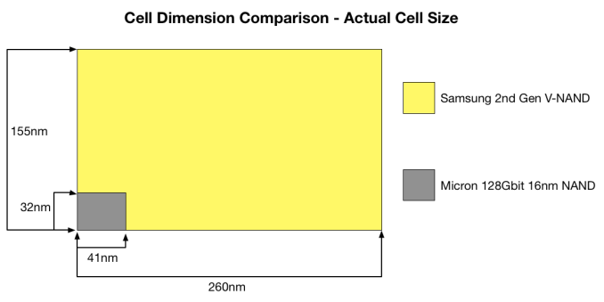
The above graph gives some guidance as to how big each cell in V-NAND really is. On the next page, I will go through the method of how cell size is really calculated and how V-NAND compares with Micron’s 16nm NAND but the above gives a good picture of the benefit that 3D NAND has. Obviously, when each cell is larger and the distance between individual cells is higher, there are more electrons to play with (i.e. more room for voltage state changes) and the cell to cell interference decreases substantially. Those two are the main reasons why V-NAND is capable of achieving up to ten times the endurance of 2D NAND.
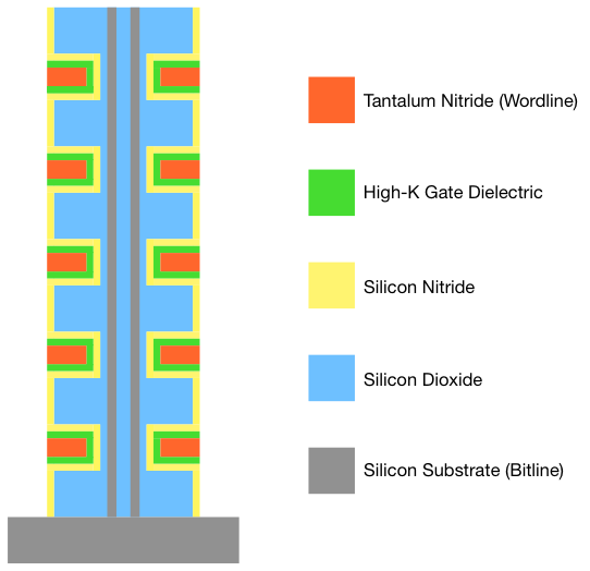
Moreover, scaling in vertical dimension does not have the same limitations as scaling in the X and Y axes do. Because the cost of a semiconductor is still mostly determined by the die area and not by the height, there is no need to cram cells very close to each other. As a result, there is very little interference between the cells even in the vertical direction. Also, the usage of high-K dielectrics means that the control gate does not have to wrap around the charge trap. The result is that there is a hefty barrier of silicon dioxide (which is an insulator) between each cell, which is far more insulating than the rather thin ONO layer in 2D NAND. Unfortunately, I do not know what is the exact distance between each cell in the vertical dimension but I think it is safe to assume that it is noticeably more than the ~20nm in 2D NAND since there is no need for aggressive vertical scaling.
As for how far Samsung believes their V-NAND can scale, their roadmap shows a 1Tbit die planned for 2017. That is very aggressive because it essentially implies that the die capacity will double every year (256Gbit next year, 512Gbit in 2016 and finally 1Tbit in 2017). The most interesting part is that Samsung is confident that they can do this simply by increasing the layer count, meaning that the process node will stay at 40nm.


160 Comments
View All Comments
Cerb - Tuesday, July 1, 2014 - link
As soon as it is cheap enough. But, don't get your hopes up about performance. SD cards are mostly limited by the controllers being slow, and in the tiny package they fit in, with the narrow margins they have, there's not a lot of room, physically and economically, to give them fast controllers, even if you get a big one that must have several NAND dies, and are talking about full-size SD, where multiple channels might be viable. It sucks, and I dislike shopping for SD cards as much as anybody, but today, that's how it is.frenchy_2001 - Tuesday, July 1, 2014 - link
I think he was talking about V-NAND (3D cells) which is independent of the controller.I would guess it will, as density will continue to scale up which will make it the cheaper technology.
It is cutting edge now, but will let Samsung scale higher densities very aggressively in the coming years, replacing all their 2D NAND production (they announced it when presenting the 3D cells).
Harry Lloyd - Tuesday, July 1, 2014 - link
Personally I have no interest in this kind of performance, and I really hope they focus on reducing prices and increasing capacities. The MX100 is just great for home usage (system and gaming), and I would like to see a 512 GB equivalent for around 100 $ by the end of 2015.Spatty - Tuesday, July 1, 2014 - link
"Oftentimes when cell size is discussed, it is only the actual size of the cell that is taken into account, which leaves the distance between cells out of the conclusion."Incorrect. Oftentimes what is being discussed is the half pitch. The 16nm, 19nm, 20nm, etc of the die. That is not the cell. The cell is Always defined as the repeatable structure in a memory device, and this includes the space between cells as described. The cell size is incorrectly referenced as being the half pitch.
Then there is marketing gimmick by companies who call their products 19nm when it is really 19nm by 2xnm. A rectangle and not a true 19nm square half pitch.
Larry Endomorph - Tuesday, July 1, 2014 - link
Good review. Bad charts. All of these are useless to color blind people:http://images.anandtech.com/doci/8216/NAND%20overv...
http://images.anandtech.com/doci/8216/cell%20inter...
http://images.anandtech.com/doci/8216/V-NAND_1.png
http://images.anandtech.com/doci/8216/850%20Pro%20...
http://images.anandtech.com/doci/8216/850%20Pro%20...
http://images.anandtech.com/doci/8216/850%20Pro%20...
http://images.anandtech.com/doci/8216/850%20Pro%20...
http://images.anandtech.com/doci/8216/850%20Pro%20...
http://images.anandtech.com/doci/8216/850%20Pro%20...
http://images.anandtech.com/doci/8216/850%20Pro%20...
http://images.anandtech.com/doci/8216/850%20Pro%20...
Cerb - Tuesday, July 1, 2014 - link
I never paid much attention, but you're right. If they changed the point shapes, and maybe dashed a couple of the lines, they could take care of that easily.fokka - Tuesday, July 1, 2014 - link
it's great to see a new drive from samsung and even greater seeing them advancing ssd tech and performance in such substantial ways. keeping that in mind i'm not really surprised about the msrp sammy is asking for its drives. and as always when new devices hit the scene, we're comparing msrp with real market prices here, so the difference should be a bit lower in a couple weeks when enough stock is available.that said, even if sata3 remains the most important storage interface today, it's kind of a shame seeing such a beautiful drive limited by this "old" interface. i know the new standards like m2, sata3.2 and pci-e-drives are still kind of a mess, but we already saw what higher throughputs in combination with more efficient interface protocols can do and seeing an expensive enthusiast drive like the 850 pro connected to sata3 just makes it seem more limited than it needed to be.
all that said, it doesn't change much for the average user, or advanced users even, since for most people a good sized evo or crucial is all they ever need in the years to come. upgrading to expensive drives like the 850 will only make sense for the most demanding users, for the rest it will only get interesting again when pci based storage gets more affordable.
Daniel Egger - Tuesday, July 1, 2014 - link
Minor nit: There's no such thing as "pentalobe torx" it's either one or the other but I'm guessing that it might have been torx security since pentalobe screws have only been used by Apple a couple of years back.iwod - Tuesday, July 1, 2014 - link
Its great to see its doing well in power consumption area. Which is important in Notebook. I hope we could bring this down to 2W or even 1.5W during operation.I really do think our SSD storage tier deserve a PCI-E lane direct from CPU. It would be great if the market just settle on 2x PCI-E 3.0 from CPU. We get 2GB/s out of it. That is plenty of headroom to grow until we move to PCI-E 4.0
hojnikb - Tuesday, July 1, 2014 - link
Thats what sata-express is doing