Imagination's PowerVR Rogue Architecture Explored
by Ryan Smith on February 24, 2014 3:00 AM EST- Posted in
- GPUs
- Imagination Technologies
- PowerVR
- PowerVR Series6
- SoCs
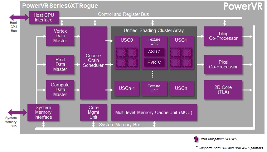
Imagination’s PowerVR Rogue Series 6/6XT USCs Dissected
Diving right into the heart of the matter, it’s probably best to start with a partial explanation for why Imagination is being so forward about their architecture after all this time.
Imagination’s principle blog, Graphics cores: trying to compare apples to apples, opens up with an argument over just what a “core” is and how it should be counted. Imagination doesn’t name any names, but from the context of their blog it’s clear that they’re worried about being in a core war and losing based on who’s counting cores and how. Time and time again we’ve seen chip and device makers promote their products both by their clockspeeds and their number of cores, leading to both MHz wars and core wars.
Both of these pieces of data are in fact absolutely essential to understanding a product, but consumers – rightfully disinterested in needing a Comp. Engineering degree to understand their purchases – will latch on to one or both numbers, which in turn rewards whoever can push a product with the highest clockspeed or the highest number of cores. The latter in turn can result in some very creative accounting, such as the Motorola X8, where components that aren’t traditionally called a core end up in the core count.
In the SoC GPU space there thankfully isn’t any creative accounting going on, but the nature of the Rogue architecture combined with Imagination’s previous method of counting cores has left Imagination shooting themselves in the foot if they were to get into a core war. If nothing else, the fact that Imagination has previously uses the term “core” to define a single USC, which depending on the specific design may be replicated several times, means that they end up having relatively low core counts.
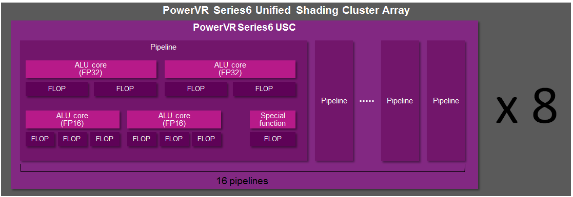
Compounding that matter is that at a pipeline or shader core level (there’s that word again), Rogue has several FP32 (or FP16) ALUs when other architectures may only have one. So even if one were to count pipelines, Imagination would come up with just 16 cores in a USC.
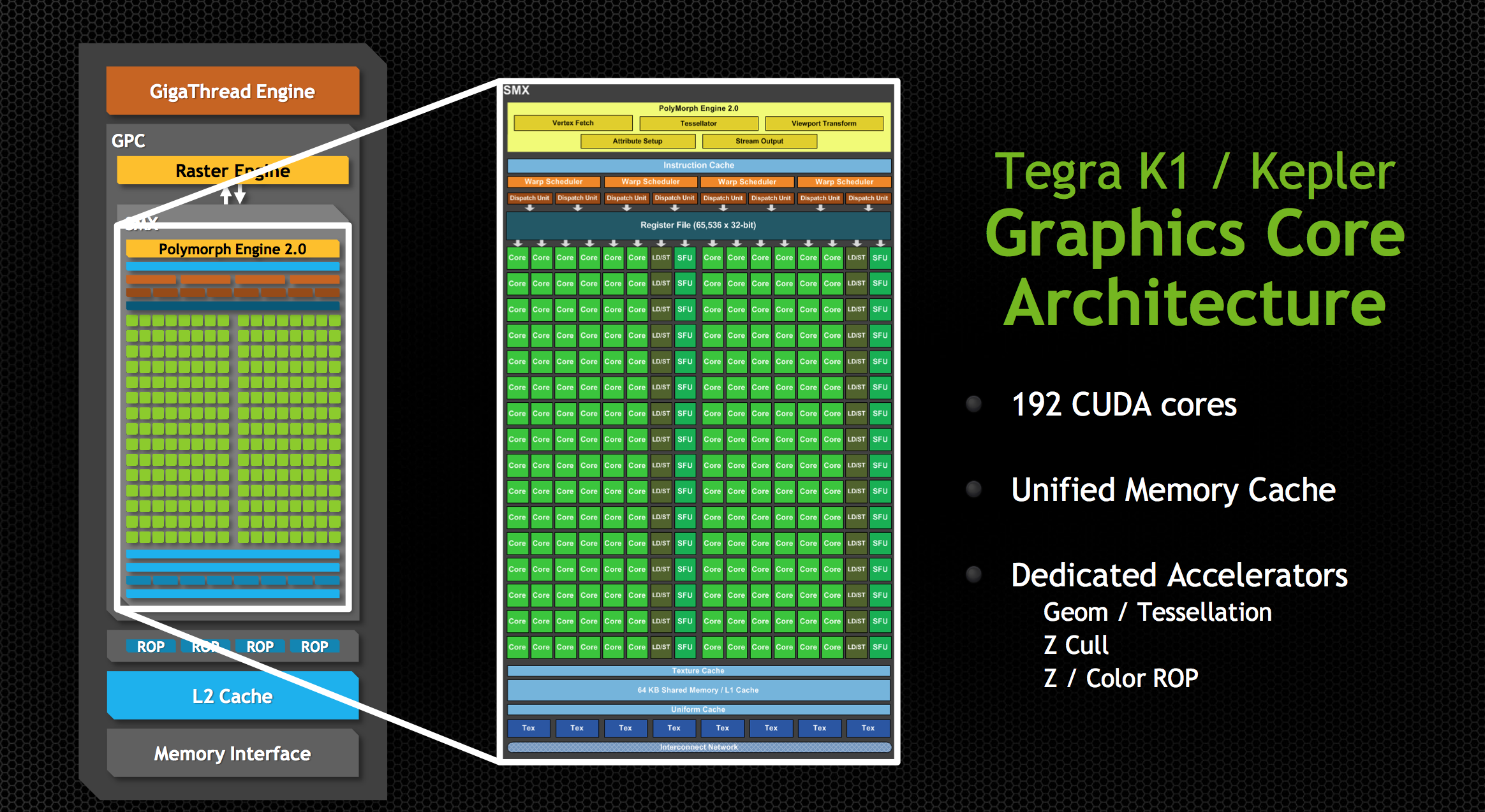
Their competition and impetus – and again Imagination hasn’t named any names – would appear to be NVIDIA, who just recently announced their Tegra K1 SoCs. A K1 contains 192 CUDA cores, each much narrower than a Rogue pipeline. So even though a high-end Rogue design would have 6 or so USCs, that would only be 96 pipelines versus 192 CUDA cores. Imagination clearly doesn’t want to be dismissed based on this metric, hence their interest in arguing what a core is, and more importantly part of the reason for their desire to open up and discuss their architecture so that we can understand why this difference matters. Imagination may only have 96 pipelines, but they have many more ALUs in each one of those pipelines.
The Rogue
And that brings us to the Rogue architecture. For today’s article and blog releases, Imagination has given us some surprisingly deep details on the Rogue USC, from which we can finally paint a picture of how thread execution works on Rogue, and furthermore gather some idea on what Rogue’s strengths are and what weaknesses it faces.
We’ll begin with differentiating between Rogue as in PowerVR Series 6, and Series 6XT. Series 6XT was the recently announced refresh for the Series 6 family, intending to further improve on PowerVR performance by undertaking several optimizations to the design. At the time of that announcement we didn’t have very many details on what those optimizations were, and now we have a much better idea.

It turns out that Imagination has been doing some tinkering under the hood, and while the number of FP32 slots remains unchanged, the FP16 slots have been altered. Wait, did we say FP16 slots?! Oh yes!
It’s a shame we don’t have such similar low level details for other SoC architectures, but from a PC perspective it’s extremely interesting that Imagination has FP16 slots. As a quick refresher, on the PC side GPUs have been using FP32 operations exclusively for quite some time, and all ALUs have been FP32 for years. But of course mobile trails PC in functionality and shader complexity, so while FP16 usage is rarer in PC games and applications, it can be very common in the mobile space.
The tradeoff of course is performance for accuracy. A 16bit floating point number is pretty imprecise – a 16bit value only gives us 65K combinations – hence it’s rarely used in the PC space in favor of far more accurate 32bit floating point numbers, which offer 4 billion combinations. But a 16bit value is smaller than a 32bit value, requiring less memory to store, less bandwidth to move, less energy to compute, and fewer transistors to operate on. So in the mobile space FP16 is still in use, both on the software side and the hardware side, with developers taking care not to let the lower precision cause rendering errors.
The interesting part on the hardware side is the implementation of dedicated FP16 units, versus just running the values on FP32 units. In the PC space we do the latter, but of course FP16 operations are relatively rare. The catch being that it’s not the most efficient way to execute FP16 operations; we’re firing up a lot of extra transistors and burning extra power to do it. In the PC space this is a reasonable tradeoff, but in the mobile space it’s clear the Imagination has decided otherwise.
The end result being that Rogue has dedicated FP16 units, not unlike how NVIDIA has dedicated FP64 CUDA cores on their desktop architectures. FP16 units take up additional die space – you have to place them alongside your FP32 units – but when you need to compute an FP16 number, you don’t have to fire up a more expensive FP32 unit to do the work. Hence the inclusion of FP16 units is a tradeoff between die size and performance, with the additional performance coming from the reduction in power consumption and heat when operating on FP16 values.
That little segue aside, let’s get back to the difference between Series 6 and Series 6XT. With Series 6, Imagination has an interesting setup where their FP16 ALUs can process up to 3 operations in one cycle.
As a refresher, for a more traditional ALU we say that one ALU can achieve 2 FLOPs in one cycle because we typically count the most dense operation, the Multiply Addition (MAD), otherwise seen as a Multiply Accumulate (MAC) or Fused Multiply Addition (FMA). MAD is a special case where one ALU can do the multiply and the accumulate in one cycle, one of a handful of scenarios where multiple operations can occur at once. MADs and their variants are relatively common in graphics work, hence for GPU performance this is the number we usually quote as it’s especially useful in graphics, and being the bigger number it also makes manufacturers happier, too.
With that said, Imagination’s FP16 ALUs are more intricate than their FP32 ALUs, especially under Series 6. Unfortunately Imagination is unable to share the complete details with us of why this is (as we've noted before, they’re not yet fully open), but it’s clear from this diagram that the Series 6 FP16 ALU has been optimized for some kind of 3 operator instruction. What that operation is we don’t know, but presumably it was important enough for Imagination to give their FP16 ALUs the ability to do it in one cycle.
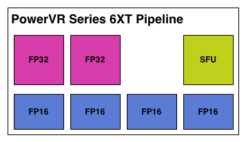
But from the perspective of an individual pipeline it’s interesting to see that with Series 6XT Imagination has shaken things up by "adding" 2 more FP16 ALUs. Keeping in mind that these are logical diagrams and not physical diagrams – in reality these ALUs are almost certainly tied together in a limited fashion rather than standing alone – Imagination has changed it so that Series 6XT can process more 2 operator FP16 instructions such as MAD. Without more details it’s hard to say for sure what’s going on, but if these “new” FP16 ALUs are really just modifications of the old FP16 ALUs, then it would be a safe assumption that Imagination can still execute their 3 operator instructions over what’s logically 2 ALUs, making these new FP16 ALUs a wider variant of the previous ALU.
Otherwise from this point of view Series 6 and Series 6XT are nearly identical. We have the 2 FP32 ALUs, and then for special functions – transcendentals and the like – a dedicated special function unit exists off to the side. On that note, for the rest of this article we will primarily be focusing on Series 6XT since it’s the newer architecture, but with the exception of FP16 operations it will be equally applicable to both Series 6 and 6XT.


95 Comments
View All Comments
grahaman27 - Monday, February 24, 2014 - link
Because apple can't have all the cool stuff!CiccioB - Monday, February 24, 2014 - link
Architecture wise, PowerVR seems more alike AMD's VLIW then nvidia's Kepler (or G200 or Fermi or Maxwell).That means PowerVR is going to have the same issues AMD had with VLIW and general computing performances and ILP.
There are also many interesting facts that could be analysed:
1. AMD went from having 5 computing ALUs to 4 to improve efficiency before switching to a completely new architetecture (CGN). PowerVR went from 5 to 7 ALUs (if we consider them all as separate units, are you sure it can process 16bit instructions togheter with 32bits one and not that those 32bits units can each execute 2x16bits instructions alternatively?)
2. PowerVR is using the same marketing politics used by AMD to count their computing core. They showed they had more computing core than nvidia competitor's architecture, but in the end, for the fact that they couldn't keep all of them feeded, they were less efficient.
3. nvidia passing from Kepler desktop to Kepler mobile removed ROPs and TMU. So, probably they think their architetcure (and GPUs on mobile in general) are less bottlenecked under those terms. PowerVR went incresing them, so they possibly think ROPs and TMU are more important then shaders... which is which? Both of them are trying to hide some deficiency of their respective architetcture?
4. We do not really know anything about PowerVR geometry power. nvidia in Kepler SMX has special function units (polymorph engine) that is connected directly to the shaders. That seems to give a enormous boost to geometric performaces (expecially tesselation) that rightly scale with the number of active SMX. PowerVR seems to have chosen AMD implementation with off-computational-core tesselator that do not scale automatically. How's going to behave PowerVR with future games that may need more geometric performances?
5. Again, as someone altready asked, tile based rendering was used on the desktop but was soon abandoned as it could not give any real advantages over the raw power of other architectures that grew much faster that what PowerVR could optimize their algorithms, making tile based rendering less and less profitable. What makes that scenario different that what we are witnessing in this period where mobile resolutions are growing to be even bigger than desktop monitors and that games complexity is gonig to increase for the arrival of these really powerful GPUs (K1 in primis)?
6. We lack the die area occupation comparison. How big is a 6 modules Rogue with respect to nvidia K1? If it is, just to say, twice nvidia die area, that would be a problem even thought the power consumption is the same. If it half, that would mean that PowerVR could make double K1 perfomance (if we believe Rogue 192 shaders perform like Kepler 192 ones). That would mean nvidia is in trouble just before beginning the high end socket race.
7. It seems PowerVR is behaving a bit like 3DFx did at the time, till it died. They were using their advanced but old technology to the exterme, so they rendered at 16bit instead of 32, used 16bit Zbuffer instead of 24 and many more "tricks" that were forced to try to hide what was quite clear: 3DFX didn't have the right architecture to compete with new companies like nvidia and ATI that started their story with the right step and much more powerful architectures (TNT2 simply destroyed Voodoo3 under all points, and beware, I was an Voodoo3 unfortunate owner). Will PowerVR go the same end trying to force the use of obsolete technics while all the others competitors are clearly pointing to constantly increasing raw power with no trade-offs (or with minimal ones?)
DanNeely - Monday, February 24, 2014 - link
AMDs shift from VLIW5 to VLIW4 was driven by the decline of DX9. DX9 was explicitly designed around a 5 step path; VLIW5 was tied directly to that. DX10's more flexible workflow rarely allowed for a 5 wide execution path.For VLIW4 AMD tied functional units together more than Imagination appears to've done here. They have 4 normal ALUs that match with the 4x 16bit ALUs in Rouge; but to do a special function operation they used 3 of the 32bit ALUs instead of using dedicated hardware. The tradeoff was that a special function cost a lot more normal processing capacity than it did before. Power VR doesn't appear to have put enough general purpose computing power place to do the same, and is required to use a dedicated SFU by default (even assuming they felt the tradeoff was worth like AMD does).
The main thing I'm curious about is if the 16 and 32bit ALUs are separate hardware; or if they implemented them similar to how SSE/AVX are done on x86 where the same hardware can do 2 32 (16) bit or 1 64 (32) bit operation.
http://www.anandtech.com/show/4061/amds-radeon-hd-...
Ryan Smith - Monday, February 24, 2014 - link
"The main thing I'm curious about is if the 16 and 32bit ALUs are separate hardware; or if they implemented them similar to how SSE/AVX are done on x86 where the same hardware can do 2 32 (16) bit or 1 64 (32) bit operation."They're separate hardware. Just as how NVIDIA uses separate FP32 and FP64 CUDA cores.
ryszu - Monday, February 24, 2014 - link
We're nothing like VLIW4/5, mobile Kepler still has ROPs and texture hardware, the area is absolutely nowhere near where you think it is and the architectural features we have in the front-end remain class leading and entirely sensible for mobile.CiccioB - Monday, February 24, 2014 - link
Sorry, maybe I was not that clear. I didn't meant they removed completely ROPs and TMUs, I was hinting to the fact that they decreased their number in a SMSX for mobile with respect to a SMX for desktop. ROPs are tied to memory channel, and that may be the cause. But TMUs are not, so they could be the same number as they are in desktop implementation.It seems nvidia sees those many ROPs and TMUs bottlenecked by RAM bandwidth so they spare space and power by not adding them.
PowerVR on the contrary has a ROPs and TMUs ratio with respect to shaders (or computing core) that is much higher. One or the other took the wrong assumption (also tied to the memory controller width, that may be higher as you want but costs in terms of die size and power). I'm curious to know who made it.
ryszu - Monday, February 24, 2014 - link
Ah, I see. Our ALU:TEX:ROP is different to Kepler (and again to Maxwell), yes. We're focused on still being strong for the basics (texturing, pixel fill) while still having a lot of shading to go with it. I can't speak for NV's design choices, just that both have pros and cons depending on market.The rest of your comment still has a lot of problems in respect to the PowerVR Rogue architecture and how it works, how it works in mobile, and how it compares to K1 and pre-GCN AMD.
Ryan Smith - Monday, February 24, 2014 - link
"Architecture wise, PowerVR seems more alike AMD's VLIW then nvidia's Kepler (or G200 or Fermi or Maxwell).That means PowerVR is going to have the same issues AMD had with VLIW and general computing performances and ILP."
To be honest I had the same thought at first. We've known that Rogue has multiple slots per pipeline since the Apple A7 came out, so when I first heard that I had the same thought. Given the greater simplicity of mobile SoCs, it would certainly make sense.
That said, after finally having access to IMG's technical details, it's clear to me that this is not the case, which was part of the reason I was so excited to work on this article. It's sort of like Fermi and it's sort of like VLIW5, but in reality it's neither.
The most important point is that in AMD's VLIW designs they had 4/5 ALUs all alike (for the sake of this discussion we'll ignore the T-unit). So to maximize a Streaming Processor's utilization, you needed to be able to extract a full 4-5 instructions of ILP out of a thread. Which was easy to do under DX9 (RGBA + lighting) and a lot harder to do under DX10.
Rogue on the other hand doesn't have ILP requirements nearly as high due to the fact that the 6 ALUs are not identical and are rarely all going to be in use at once (we don't even count the FP16 units in our GFLOPs calculations). They do have ILP requirements, unlike GCN, but for FP32 it's only 2 instructions for the 2 FP32 ALUs. This is in fact rather similar to Kepler (but not Maxwell) in that NVIDIA has a similar reliance on ILP to keep all of their CUDA cores fed. Half of the threads on Kepler need to co-issue another FP32 op to fill the other 64 CUDA cores in an SMX; Rogue is a bit worse in this regard since every thread needs to co-issue to fill every second FP32 ALU.
FP16 on the other hand is trickier, since that's a full 4 ALU setup. Worst case scenario is that IMG needs to pull off 4 instructions of ILP to maximize their utilization, but this is a bit murkier since we don't know why Series 6 had the unusual 3 operator FP16 ALUs in the first place. As such I'm less familiar with where FP16 is being used in mobile today, so it's harder to draw comparisons for what FP16 utilization may be like. That said, there's also the unknown of die size and power requirements of using FP16 units for FP16 math versus using FP32 units for the same task. I'm not sure if IMG has reason to be worried about FP16 utilization if they can pack 2x as much hardware in the same die size and power envelope.
Ultimately I'd classify Rogue as being closer to Fermi/Kepler than VLIW, which is why those are the comparisons we went with in the article. The 2 wide FP32 pipeline isn't nearly as narrow as AMD's VLIW, and the instructions themselves aren't the inflexible chaos that was VLIW as a language.
"Again, as someone altready asked, tile based rendering was used on the desktop but was soon abandoned as it could not give any real advantages over the raw power of other architectures that grew much faster that what PowerVR could optimize their algorithms, making tile based rendering less and less profitable. What makes that scenario different that what we are witnessing in this period where mobile resolutions are growing to be even bigger than desktop monitors and that games complexity is gonig to increase for the arrival of these really powerful GPUs (K1 in primis)?"
One of the problems IMG faced in the old days was that DirectX and Windows weren't very well suited for their TBDR design; they pretty much had to fight the API at times to get what they wanted. For iOS/Android it's difficult to draw comparisons - though I'd note iOS has always been driven by IMG GPUs and hence always used TBDR - but Windows for its part has since gotten much better. In particular there are API hooks to allow applications to see if the GPU is TBDR. I'm not sure if that's enough, but it does mean things have changed at least a little bit since the old days.
Scali - Monday, February 24, 2014 - link
In D3D11 there is now a flag to indicate whether you are running on a TBDR device or not: http://msdn.microsoft.com/en-us/library/windows/de...CiccioB - Monday, February 24, 2014 - link
I didn't realize that in counting those GFlops you ignored the 16bit ALUs, Issuing two instructions should be much easier than issuing 3, 4 or even 5, not to speak about 6 or 7.However I bet that PowerVR next architecture (or the next one again) will remove those 16bit ALUs and will introduce a couple of them able to issue 32 OR 2x16bit instruction, so that they can pack more shaders in the same area.
About TBDR design... the alternative to DirectX is OpenGL. Is it more suited for TBDR architecture than "brute force" ones?
Still I perceive PowerVR architecture as something from the past that has survived to to now until the big one have entered the mobile game for real. Kepler is a very efficient architecture and Maxwell has demonstrated that it can be even better. How is PowerVR going to fight against an architecture as flexible as nvidia ones that can also be used for CUDA computing and thus being adopted into markets (and for other tasks) PowerVR cannot with their current architecture? Not to forget that nvidia can now easily bring to their mobile versions whatever engine exists for their desktop GPUs.
Will extreme (but not so flexible) efficiency win against something not that efficient but able to do much more things in a easier way?
Would mobile game engines bet more on computing shaders power or memory bandwidth?
Will new DX10/DX11-alike engines (whose features are supported by new architectures) still be TBDR friendly? Does TBDR design still scale for the modern ultra high resolution displays or as for desktops "brute force" (or simply more power more performance) will rule out?
I think this year will tell us very much.