AMD Kaveri Review: A8-7600 and A10-7850K Tested
by Ian Cutress & Rahul Garg on January 14, 2014 8:00 AM ESTLlano, Trinity and Kaveri Die: Compared
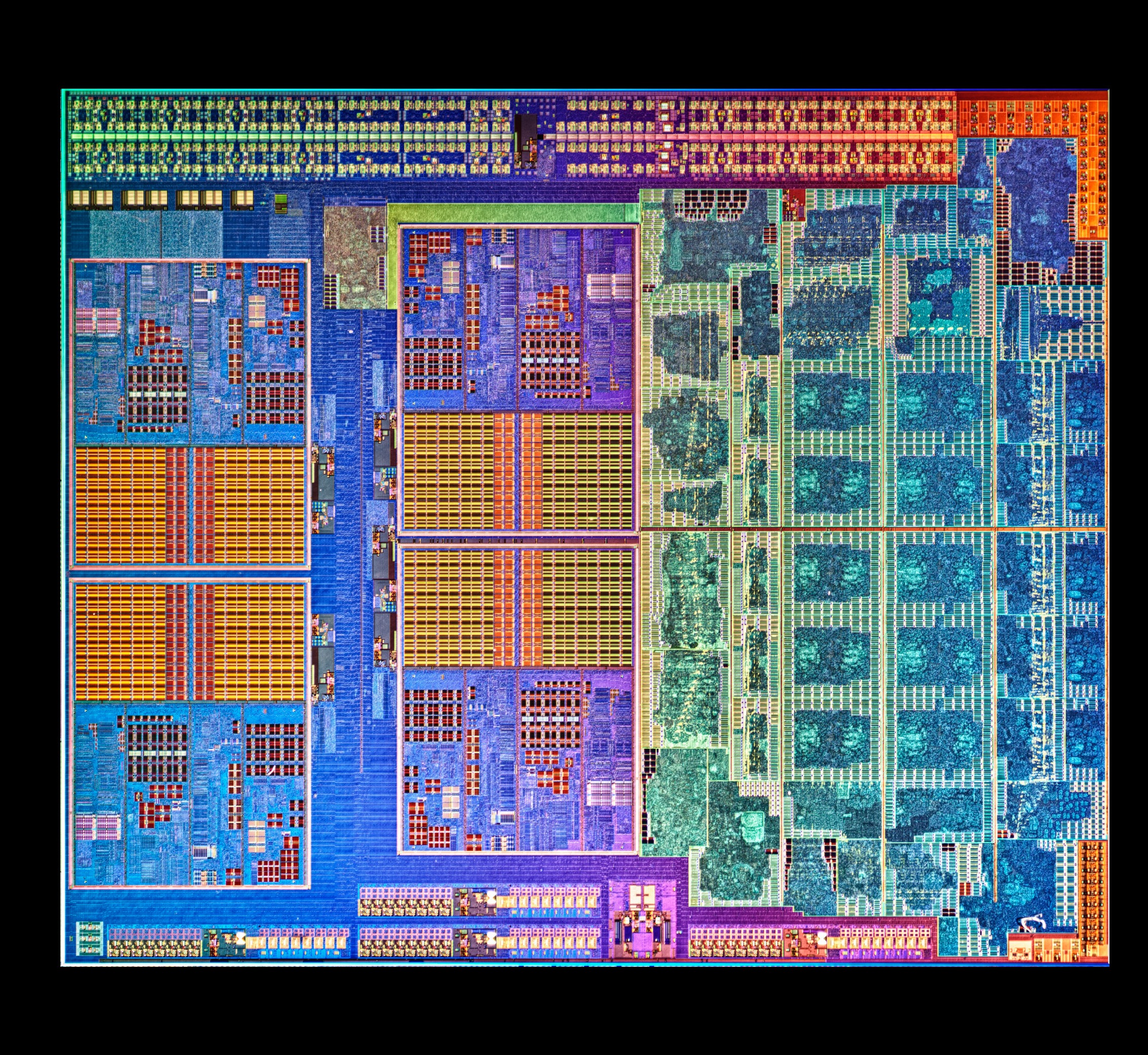
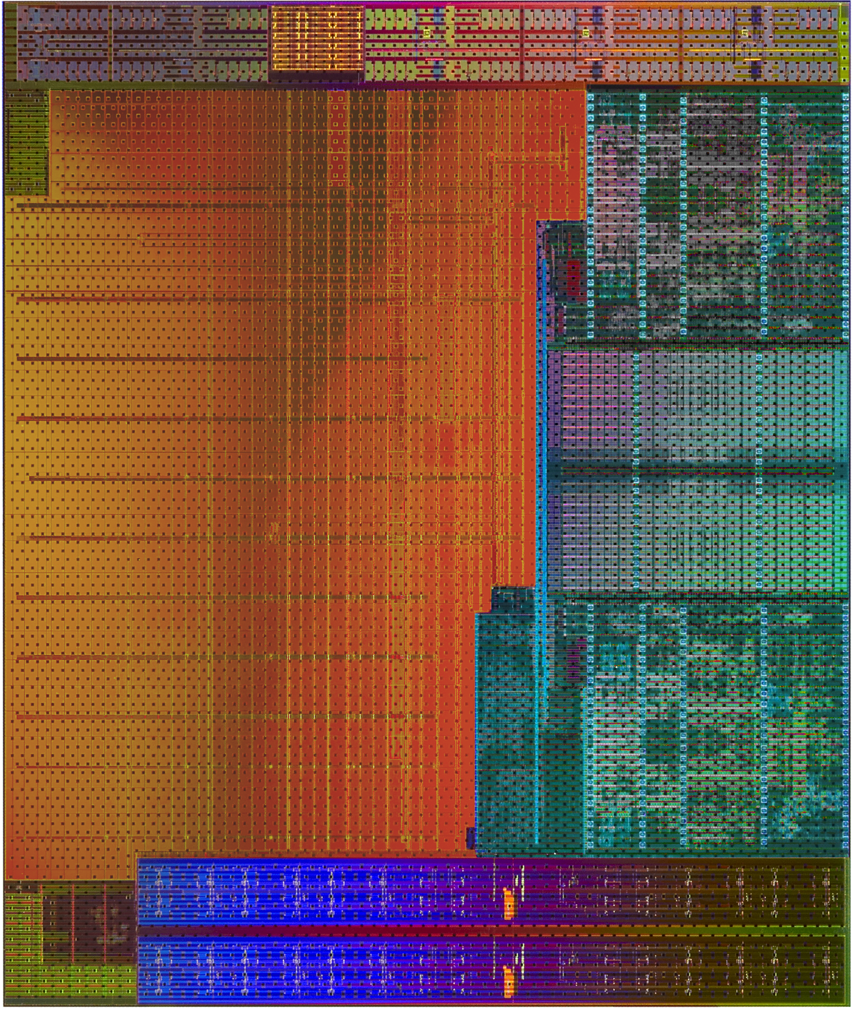
AMD sent along a high res shot of Kaveri's die. Armed with the same from the previous two generations, we can get a decent idea of the progression of AMD's APUs:
Llano, K10 Quad Core

Trinity and Richland Die, with two Piledriver modules and processor graphics
Kaveri, two modules and processor graphics
Moving from Llano to Trinity, we have the reduction from a fully-fledged quad core system to the dual module layout AMD is keeping with its APU range. Moving from Richland to Kaveri is actually a bigger step than one might imagine:
| AMD APU Details | ||||
| Core Name | Llano | Trinity | Richland | Kaveri |
| Microarch | K10 | Piledriver | Piledriver | Steamroller |
| CPU Example | A8-3850 | A10-5800K | A10-6800K | A10-7850K |
| Threads | 4 | 4 | 4 | 4 |
| Cores | 4 | 2 | 2 | 2 |
| GPU | HD 6550 | HD 7660D | HD 8670D | R7 |
| GPU Arch | VLIW5 | VLIW4 | VLIW4 | GCN 1.1 |
| GPU Cores | 400 | 384 | 384 | 512 |
| Die size / mm2 | 228 | 246 | 246 | 245 |
| Transistors | 1.178 B | 1.303 B | 1.303 B | 2.41 B |
| Power | 100W | 100W | 100W | 95W |
| CPU MHz | 2900 | 3800 | 4100 | 3700 |
| CPU Turbo | N/A | 4200 | 4400 | 4000 |
| L1 Cache |
256KB C$ 256KB D$ |
128KB C$ 64KB D$ |
128KB C$ 64KB D$ |
192KB C$ 64KB D$ |
| L2 Cache | 4 x 1MB | 2 x 2 MB | 2 x 2 MB | 2 x 2 MB |
| Node | 32nm SOI | 32nm SOI | 32nm SOI | 28nm SHP |
| Memory | DDR-1866 | DDR-1866 | DDR-2133 | DDR-2133 |
Looking back at Llano and Trinity/Richland, it's very clear that AMD's APUs on GF's 32nm SOI process had a real issue with transistor density. The table below attempts to put everything in perspective but keep in mind that, outside of Intel, no one does a good job of documenting how they are counting (estimating) transistors. My only hope is AMD's transistor counting methods are consistent across CPU and GPU, although that alone may be wishful thinking:
| Transistor Density Comparison | ||||||||
| Manufacturing Process | Transistor Count | Die Size | Transistors per mm2 | |||||
| AMD Kaveri | GF 28nm SHP | 2.41B | 245 mm2 | 9.837M | ||||
| AMD Richland | GF 32nm SOI | 1.30B | 246 mm2 | 5.285M | ||||
| AMD Llano | GF 32nm SOI | 1.178B | 228 mm2 | 5.166M | ||||
| AMD Bonaire (R7 260X) | TSMC 28nm | 2.08B | 160 mm2 | 13.000M | ||||
| AMD Pitcairn (R7 270/270X) | TSMC 28nm | 2.80B | 212 mm2 | 13.209M | ||||
| AMD Vishera (FX-8350) | GF 32nm SOI | 1.2B | 315 mm2 | 3.810M | ||||
| Intel Haswell 4C (GT2) | Intel 22nm | 1.40B | 177 mm2 | 7.910M | ||||
| NVIDIA GK106 (GTX 660) | TSMC 28nm | 2.54B | 214 mm2 | 11.869M | ||||
If AMD is indeed counting the same way across APUs/GPUs, the move to Kaveri doesn't look all that extreme but rather a good point in between previous APUs and other AMD GCN GPUs. Compared to standalone CPU architectures from AMD, it's clear that the APUs are far more dense thanks to big portions of their die being occupied by a GPU.


380 Comments
View All Comments
jasonelmore - Tuesday, January 14, 2014 - link
I really wish these were launching in BGA GDDR5 Laptop/Mini ITX Packages.jaydee - Tuesday, January 14, 2014 - link
Pretty much what I was thinking as well. There are two mini-ITX FM2+ motherboards available on newegg, niether are "thin", and neither have DisplayPort. AMD's opportunity here is to market it's 45W Kaveri as the best CPU/GPU for the price in a small package. They NEED to get outside of the typical ATX, micro-ATX, mini-ATX box and into SFF, have all the ports that everyone wants, be creative with packaging and configurations (like GDDR5). They will never win a war with Intel in the traditional form-factor PCs, which is a rapidly shrinking market anyways.takeship - Tuesday, January 14, 2014 - link
Agreed. Any build not restricted to half height GPUs is better off going with a cheap intel cpu & discrete card. AMD really should be targeting ultra SFF type builds where Iris Pro is thermally limited, and a dGPU isn't an option.rhx123 - Tuesday, January 14, 2014 - link
GDDR5 7750's are available half height and at a decent price point, so even in a Low Profile machine a cheap Intel + 7750 is a better option. That's what I'm running anyway. Passively cooled i3 never reaches above 65c and the Saphire 7750 Low Profile is pretty quiet at idle.Mopar63 - Tuesday, January 14, 2014 - link
The last paragraph of this article shows someone that GETS IT, where Kaveri and the APU design in general is heading.nissangtr786 - Tuesday, January 14, 2014 - link
I can't believe how right I was, I was saying i3 4130 cpu performance and 2400-2500 3dmark11 gpu performance similar to my gt650m in my laptop. Funnily enough my laptop with i5 3210m at 2.9ghz gt650m with screen takes 87w, if I had an i3 4130 it would take about 92w lets say so it is about right. I am more shocked how spot on I was.HammerStrike - Tuesday, January 14, 2014 - link
The entire Anand reader base congratulates you on your deep insight and prophetic powers of deduction.nathanddrews - Tuesday, January 14, 2014 - link
I, for one, welcome our new nissangtr786 overlord.Zorba - Tuesday, January 14, 2014 - link
It would have been nice to see some non-integrated chips added to the benchmarks like an FX-6300. Ever since the APUs came out, it seems no reviews actually compare high-end iGPU vs moderate dGPU and CPU. Looking at the price, you could get a decent CPU+GPU for the cost of the A10-7850K, so it would be nice to see that as an option.R3MF - Tuesday, January 14, 2014 - link
"do any AnandTech readers have an interest in an even higher end APU with substantially more graphics horsepower?"Yes, and No.
I do want a higher-end APU, but I'd like to see one with four CPU modules and 256 shaders:
47% of the kaveri die space is GPU
http://www.extremetech.com/wp-conten...d-to-intel....
If you consider that roughly 20% is uncore, that leaves roughly 33% as CPU.
Give or take, 8 shader cores is fifty percent larger than 4 cpu cores.
You could double that cpu portion to 66%, and still leave 14% for shader cores.
Make the total die size just 10% bigger and you have an 8 cpu core APU with 4 HSA enabled shader cores ready to grind through FPU work. pretty much die-size neutral.