NVIDIA Tegra K1 Preview & Architecture Analysis
by Brian Klug & Anand Lal Shimpi on January 6, 2014 6:31 AM ESTTegra K1 ISP & Video
NVIDIA’s Tegra K1 SoC also makes some dramatic improvements on the ISP side. We saw SoCs start arriving with two ISPs sometime in 2013, which allowed OEMs to deliver a host of new imaging experiences, like shot in shot video and simultaneous use of both front and rear cameras. With Tegra K1, NVIDIA is not only moving to two ISPs, but it’s also making ISP more of a first class citizen.
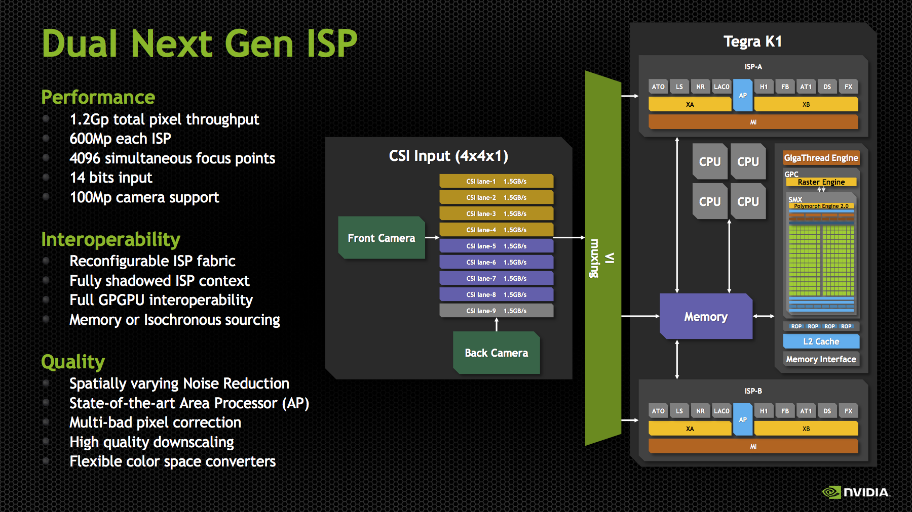
For those not familiar, ISP (Image Signal Processor) handles the imaging pipeline for still photos, video, and performs tasks like Bayer to RGB conversion (demosaicing), 3A (Autofocus, Auto Exposure, Auto white balance), noise reduction, lens correction, and so on. Although NVIDIA has always included an ISP onboard, I couldn’t shake the feeling that still imaging performance could’ve been better, especially in the few cases that allowed direct comparison (HTC One X). With Tegra K1, there’s more die area dedicated to ISP than in the past, and there are two of them to support the kind of dual camera applications that have quickly become popular.
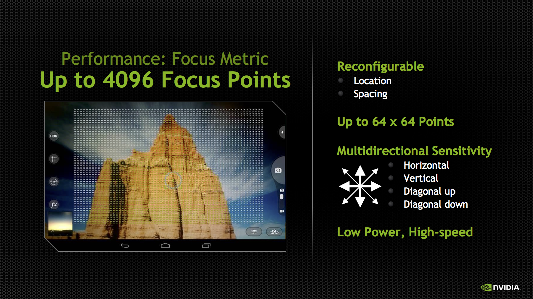
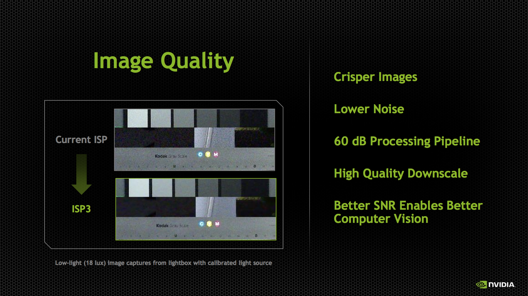
Tegra K1 includes the third generation of NVIDIA’s ISP, capable of processing 600 MP/s on each ISP with 14 bit input, and support for up to 100 MP cameras. There are two of them, so NVIDIA quotes the total pixel throughput as up to 1.2 Gp/s. This is dramatically increased from Tegra 4, which supported up to 400 Mp/s at 10 bits per pixel. In addition the K1’s ISP now supports up to 4096 focus points, a 64x64 array, for its autofocus routine. The ISP also has better noise reduction, and local tone mapping, a feature we’ve also seen become popular for combining parts of images and recovering some of the dynamic range lost with ever shrinking pixel sizes.
Tegra K1 retains compatibility with the Chimera 1.0 features that we just saw in the Tegra Note 7, like object tracking, always-on HDR, slow motion capture, and full resolution burst, and adds more. NVIDIA has kept the Chimera brand for the K1 SoC, calling it Chimera 2.0, and envisions this architecture enabling things like better temporal pixel binning (combining 8 exposures from the CMOS to drive noise down further), faster panorama, video stabilization, and even better live preview with effects applied. The high level of Chimera seems to be the same – kernels that either run on the CPU, or on the GPU (ostensibly in CUDA this time) before or after the ISP and in a variety of image spaces (Bayer or RGB depending).
On the video side, Tegra K1 continues to support 2160p30 (4K or UHD video at 30FPS) encode and decode. Broken down another way, H.264 High Profile Level 5.1 decode and 4K H.264 High Profile 4.2 encode. The fact that there’s a Kepler next door made me suspect that NVENC was used for most of these tasks, but it turns out that NVIDIA still has discrete blocks for video encode of H.264, VP8, VC1, and others. These are the same video encode and decode blocks as what were used in Tegra 4, but with some further optimizations for power and efficiency. The Tegra K1 platform includes support for H.265 video decode as well, but this isn’t accelerated fully in hardware, rather the decode is split across NVENC and CPU.
NVIDIA showed off a K1 reference board doing 4Kp30 H.264 decode on an attached display, I didn’t notice any dropped frames. Of course that’s a given considering we saw the same thing on Tegra 4, but it’s still worth noting that the SoC is capable of driving 4K/UHD displays over eDP 1.4, LVDS and HDMI 1.4b.
The full GPIO breakdown for Tegra K1 includes essentially all the requisite connectivity you’d expect for a mobile SoC. For USB there’s 3 USB 2.0 ports, and 2 USB 3.0 ports. For storage Tegra K1 supports eMMC up to version 4.5.1, and there’s PCIe x4 which can be configured


88 Comments
View All Comments
name99 - Monday, January 6, 2014 - link
This is not especially new (though it might have been in Transmeta's time).Given the existence of robust and generally accurate branch prediction, a number of architectures have been proposed that are based on checkpoints and rollbacks rather than a ROB. There are a number of ways you can slice this, with the newest, richest, ideas having names like CFP (Continuous Flow Processing) and DOE (Distributed OutOfOrder Execution), both created by folks with Intel affiliations.
What these architectures do is help you with long memory latency delays because (in spite of what the above author said) OoO doesn't help much there. OoO covers L1 delays, most L2 delays, some L3 delays if you're lucky, and very little of the main memory delay. That's why prefetching is still an active area of research (e.g. there were some minor but cute improvements to prefetch in Ivy Bridge). The problem is the length of the ROB limits how far you can cover latency in a ROB architecture, and you can't make the ROB much larger because that increases the size (and slows down) the register file. Checkpoint architectures are not constrained in this way.
HOWEVER all this is neither here nor there.
There are three interesting claims being made about Denver
- it uses a checkpoint architecture. Interesting if true, because this type of architecture has the potential to be the general replacement for ROB OoO; even if the first implementation is only equivalent of ROB OoO, there are many new optimizations it opens up
- it uses some sort of "Code Morphing". Who knows WTF this means. Could be anything from rewriting ARM assembly to an internal ISA (like Apple have done many times, from 68K->PPC to Rosetta; likewise DEC did this to run x86 binaries on Alpha) to PPro style µOps to something very minor like the way POWER "cracks" a few instructions to simpler instructions.
- it is "7-wide". If this is an issue width, it's a bullshit measure that no-one who knows anything cares about. If this is a Decode/Rename/Dispatch width, it is a major leap forward, and the only likely way it is doable at such low power is through use of a trace cache which records dependency and remap information. If nVidia has this, it would be very cool.
Given that this is nVidia, my betting would be that every one of these is underwhelming. The exciting checkpoint architecture is in fact a standard ROB (with standard ROB limitations). The code morphing is minor cracking of a few "hard" instructions. The 7-wide refers to issue width so, ho-hum.
Loki726 - Tuesday, January 7, 2014 - link
"This is not especially new."Agreed. I mainly posted it for reference in case someone had not seen it before.
Da W - Monday, January 6, 2014 - link
For that matter i would prefer a Kabini surface mini and for AMD to follow Nvidia in game streaming (from PC or from Xbox one).chizow - Monday, January 6, 2014 - link
Great write-up guys, you're right, this is the most exciting announcement I've seen in the CPU/GPU/SoC space in a very long time, similar to A7 Cyclone but 2x that due to both CPU and GPU bombshells. It's probably the first analysis I've read in full because everything was just that interesting relative to what the rest of the industry is doing.One burning question that I did not see touched upon at all, here or elsewhere:
****What does Tegra K1 do for Nvidia's Kepler IP tech licensing prospects?
It seems to me, even if Tegra itself is not a smash hit for Nvidia in terms of design wins, the GPU technology is so disruptive that even if it gets into a few major designs (Surface 3, Nexus 7 2014, Asus Transformer for example) it may very well *FORCE* the other major industry players (Intel, Samsung, Apple) that don't have their own in-house graphics IP to license Kepler to remain competitive?
What do you all think? Any buzz on that front at CES?
OreoCookie - Friday, January 10, 2014 - link
As far as I can tell, nVidia only compared the GPU performance of the A7 to Tegra K1 but not the CPU performance. I'd be very curious to see how the Denver cores compare to Apple's Cyclone cores, though.Also, given Tegra's release date, it'll compete with Apple's A8.
Krysto - Saturday, January 11, 2014 - link
Based on the (limited) technical description and how massive those cores are, along with clock speeds that are almost twice as high as what Apple typically uses, I'd say they will beat Apple's A8 (probably just an upgraded Cyclone) pretty easily - unless Nvidia did something stupid with that software translation that adds too much overhead and and cuts the performance too much.But since we don't know exactly what's going on inside of those CPU cores, we'll have to wait for more details or a direct comparison (and hopefully Denver actually arrives this fall, and not next year).
OreoCookie - Sunday, January 12, 2014 - link
Initially, I thought so, too, but knowing it's a Transmeta Crusoe-like design, I'd be much more cautious about performance. At the same clockspeed, the Crusoe was about half or a third as fast as a Pentium III. The advantage was that the cpus consumed much less power.Of course that tells us nothing of a comparison between the A7 or A8 and a Denver-based K1 other than that the architectures are not directly comparable.
name99 - Monday, January 6, 2014 - link
"We’ve seen code morphing + binary translation done in the past, including famously in Transmeta’s offerings in the early 2000s, but it’s never been done all that well at the consumer client level.
"
Actually we've seen a few different versions of it which have worked just fine.
One obvious example (not consumer, but transparent) was IBM's switch over from custom cores to POWER cores for i-Series.
More on the consumer end, Apple have been doing this for years if you use OpenCL on their products --- they convert, on the fly, a byte code version of the GPU instructions to the target GPU. And of course anything that uses a JIT, whether it's targeting Java or JS (or Dalvik for that matter) is doing a similar sort of thing.
There may be uniquely painful aspects to doing this for x86/Windows, especially 15 years ago, but I don't think Transmeta's failure tells us anything --- this mainstream-ish tech. Especially now, in a world with hypervisors, where you have a more well-defined "space" for control code to run and bring up the OS step by step.
ruthan - Tuesday, January 7, 2014 - link
Ok, they maybe have enough GPU performance in this chip on paper. But how is final TDP SOC power consumation for 64 bit piece?But if you want to have realy PS3 or Xbox performance, which was advertised / promised till original Ipad and we still arent here at all.
Other problem are game engines middleware performance, because 80% of mobile games using Unity3D engine, which in by my experience, much more HW resources greedy and inefficient (C# - has automatic garbage collection, all in Unity running in single thread, GUI performance is terrible, PhysX implementation is signle thread) that, that console developement kits.
Back into problem, GPU is maybe ok, but for final overall performance you need also CPU with desktop like performance and to freed GPU with data and im dont think so that these weak ARM is nearly here.
So in overall i dont agree with these big perfromance and desktop like performance promises at all, would be ok, but it is only empty words.
kwrzesien - Tuesday, January 7, 2014 - link
I think nVidia has finally done it with a great SoC/GPU! I hope they get a few very solid design wins, it could change alot.Looking at those beautiful chip diagrams I think they have the CPU/CPU balance just right.