NVIDIA Tegra K1 Preview & Architecture Analysis
by Brian Klug & Anand Lal Shimpi on January 6, 2014 6:31 AM ESTCPU Option 2: Dual-Core 64-bit NVIDIA Denver
Three years ago, also at CES, NVIDIA announced that it was working on its own custom ARM based microprocessor, codenamed Denver. Denver was teased back in 2011 as a solution for everything from PCs to servers, with no direct mention of going into phones or tablets. In the second half of 2014, NVIDIA expects to offer a second version of Tegra K1 based on two Denver cores instead of 4+1 ARM Cortex A15s. Details are light but here’s what I’m expecting/have been able to piece together.
Given the 28nm HPM process for Tegra K1, I’d expect that the Denver version is also a 28nm HPM design. NVIDIA claims the two SoCs are pin-compatible, which tells me that both feature the same 64-bit wide LPDDR3 memory interface.
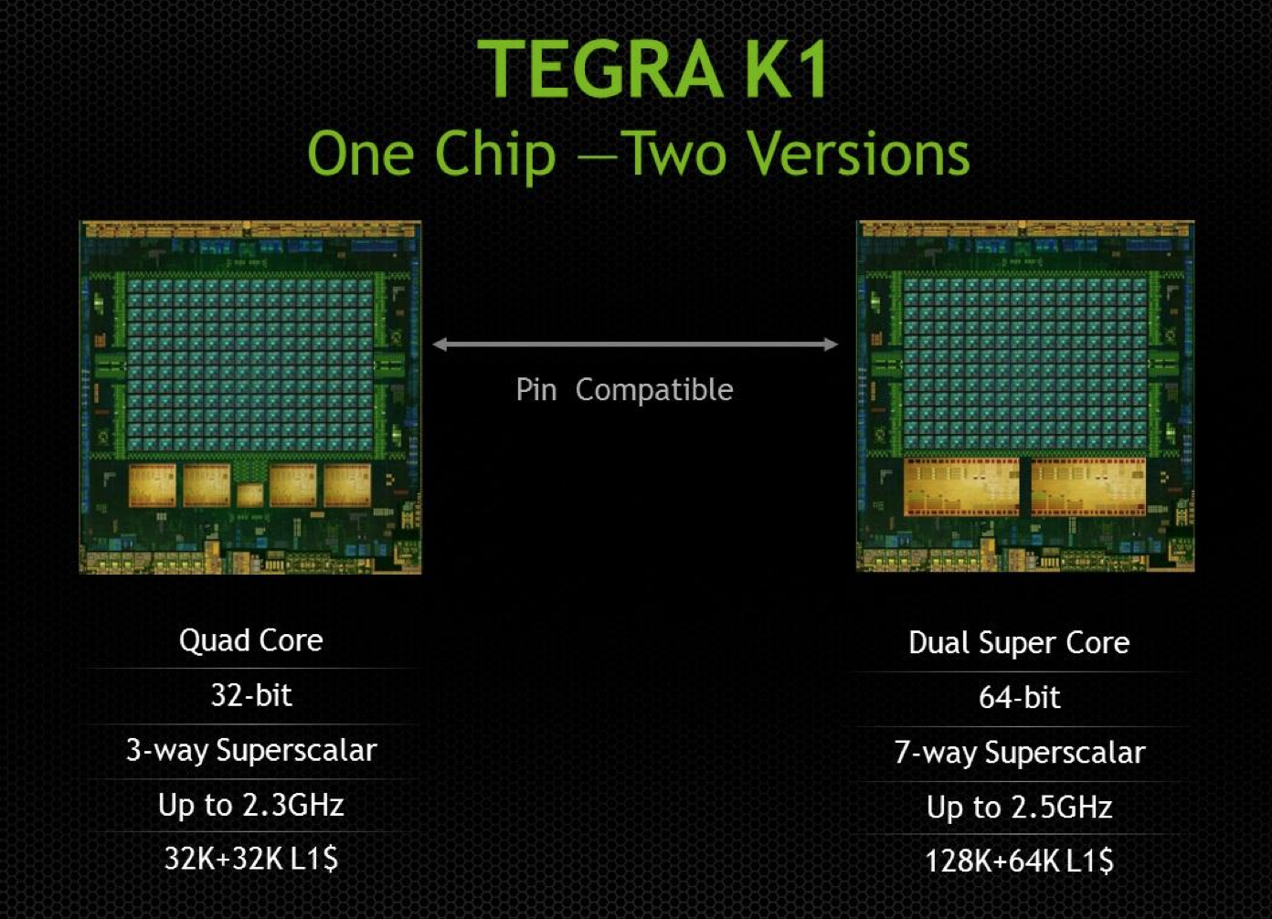
The companion core is gone in the Denver version of K1, as is the quad-core silliness. Instead you get two, presumably larger cores with much higher IPC; in other words, the right way to design a CPU for mobile. Ironically it’s NVIDIA, the company that drove the rest of the ARM market into the core race, that is the first (excluding Apple/Intel) to come to the realization that four cores may not be the best use of die area in pursuit of good performance per watt in a phone/tablet design.
It’s long been rumored that Denver was a reincarnation of NVIDIA’s original design for an x86 CPU. The rumor there being NVIDIA used binary translation to convert x86 assembly to some internal format (optimizing the assembly in the process for proper scheduling/dispatch/execution) before it hit the CPU core itself. The obvious change being instead of being x86 compatible, NVIDIA built something that was compatible with ARMv8.
I believe Denver still works the same way though. My guess is there’s some form of a software abstraction layer that intercepts ARMv8 machine code, translates and optimizes/morphs it into a friendlier format and then dispatches it to the underlying hardware. We’ve seen code morphing + binary translation done in the past, including famously in Transmeta’s offerings in the early 2000s, but it’s never been done all that well at the consumer client level.
Mobile SoC vendors are caught in a tough position. Each generation they are presented with opportunities to increase performance, however at some point you need to move to a larger out of order design in order to efficiently scale performance. Once you make that jump, there’s a corresponding increase in power consumption that you simply can’t get over. Furthermore, subsequent performance increases usually depend on leveraging more speculative execution, which also comes with substantial power costs.
ARM’s solution to this problem is to have your cake and eat it too. Ship a design with some big, speculative, out of order cores but also include some in-order cores when you don’t absolutely need the added performance. Include some logic to switch between the cores and you’re golden.
If Denver indeed follows this path of binary translation + code optimization/morphing, it offers another option for saving power while increasing performance in mobile. You can build a relatively wide machine (NVIDIA claims Denver is a 7-issue design, though it’s important to note that we’re talking about the CPU’s internal instruction format and it’s not clear what type of instructions can be co-issued) but move a lot of the scheduling/ILP complexities into software. With a good code morphing engine the CPU could regularly receive nice bundles of instructions that are already optimized for peak parallelism. Removing the scheduling/OoO complexities from the CPU could save power.
Granted all of this funky code translation and optimization is done in software, which ultimately has to run on the same underlying CPU hardware, so some power is expended doing that. The point being that if you do it efficiently, any power/time you spend here will still cost less than if you had built a conventional OoO machine.
I have to say that if this does end up being the case, I’ve got to give Charlie credit. He called it all back in late 2011, a few months after NVIDIA announced Denver.
NVIDIA announced that Denver would have a 128KB L1 instruction cache and a 64KB L1 data cache. It’s fairly unusual to see imbalanced L1 I/D caches like that in a client machine, which I can only assume has something to do with Denver’s more unique architecture. Curiously enough, Transmeta’s Efficeon processor (2nd generation code morphing CPU) had the exact same L1 cache sizes (it also worked on 8-wide VLIW instructions for what it’s worth). NVIDIA also gave us a clock target of 2.5GHz. For an insanely wide machine 2.5GHz sounds pretty high, especially if we’re talking about 28nm HPM, so I’m betting Charlie is right in that we need to put machine width in perspective.
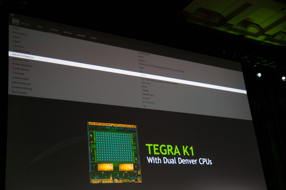
NVIDIA showed a Denver Tegra K1 running Android 4.4 at CES. The design came back from the fab sometime in the past couple of weeks and is already up and running Android. NVIDIA hopes to ship the Denver version of Tegra K1 in the second half of the year.
The Denver option is the more interesting of the two as it not only gives us another (very unique) solution to the power problem in mobile, but it also embraces a much more sane idea of the right balance of core size vs. core count in mobile.


88 Comments
View All Comments
name99 - Monday, January 6, 2014 - link
This is not especially new (though it might have been in Transmeta's time).Given the existence of robust and generally accurate branch prediction, a number of architectures have been proposed that are based on checkpoints and rollbacks rather than a ROB. There are a number of ways you can slice this, with the newest, richest, ideas having names like CFP (Continuous Flow Processing) and DOE (Distributed OutOfOrder Execution), both created by folks with Intel affiliations.
What these architectures do is help you with long memory latency delays because (in spite of what the above author said) OoO doesn't help much there. OoO covers L1 delays, most L2 delays, some L3 delays if you're lucky, and very little of the main memory delay. That's why prefetching is still an active area of research (e.g. there were some minor but cute improvements to prefetch in Ivy Bridge). The problem is the length of the ROB limits how far you can cover latency in a ROB architecture, and you can't make the ROB much larger because that increases the size (and slows down) the register file. Checkpoint architectures are not constrained in this way.
HOWEVER all this is neither here nor there.
There are three interesting claims being made about Denver
- it uses a checkpoint architecture. Interesting if true, because this type of architecture has the potential to be the general replacement for ROB OoO; even if the first implementation is only equivalent of ROB OoO, there are many new optimizations it opens up
- it uses some sort of "Code Morphing". Who knows WTF this means. Could be anything from rewriting ARM assembly to an internal ISA (like Apple have done many times, from 68K->PPC to Rosetta; likewise DEC did this to run x86 binaries on Alpha) to PPro style µOps to something very minor like the way POWER "cracks" a few instructions to simpler instructions.
- it is "7-wide". If this is an issue width, it's a bullshit measure that no-one who knows anything cares about. If this is a Decode/Rename/Dispatch width, it is a major leap forward, and the only likely way it is doable at such low power is through use of a trace cache which records dependency and remap information. If nVidia has this, it would be very cool.
Given that this is nVidia, my betting would be that every one of these is underwhelming. The exciting checkpoint architecture is in fact a standard ROB (with standard ROB limitations). The code morphing is minor cracking of a few "hard" instructions. The 7-wide refers to issue width so, ho-hum.
Loki726 - Tuesday, January 7, 2014 - link
"This is not especially new."Agreed. I mainly posted it for reference in case someone had not seen it before.
Da W - Monday, January 6, 2014 - link
For that matter i would prefer a Kabini surface mini and for AMD to follow Nvidia in game streaming (from PC or from Xbox one).chizow - Monday, January 6, 2014 - link
Great write-up guys, you're right, this is the most exciting announcement I've seen in the CPU/GPU/SoC space in a very long time, similar to A7 Cyclone but 2x that due to both CPU and GPU bombshells. It's probably the first analysis I've read in full because everything was just that interesting relative to what the rest of the industry is doing.One burning question that I did not see touched upon at all, here or elsewhere:
****What does Tegra K1 do for Nvidia's Kepler IP tech licensing prospects?
It seems to me, even if Tegra itself is not a smash hit for Nvidia in terms of design wins, the GPU technology is so disruptive that even if it gets into a few major designs (Surface 3, Nexus 7 2014, Asus Transformer for example) it may very well *FORCE* the other major industry players (Intel, Samsung, Apple) that don't have their own in-house graphics IP to license Kepler to remain competitive?
What do you all think? Any buzz on that front at CES?
OreoCookie - Friday, January 10, 2014 - link
As far as I can tell, nVidia only compared the GPU performance of the A7 to Tegra K1 but not the CPU performance. I'd be very curious to see how the Denver cores compare to Apple's Cyclone cores, though.Also, given Tegra's release date, it'll compete with Apple's A8.
Krysto - Saturday, January 11, 2014 - link
Based on the (limited) technical description and how massive those cores are, along with clock speeds that are almost twice as high as what Apple typically uses, I'd say they will beat Apple's A8 (probably just an upgraded Cyclone) pretty easily - unless Nvidia did something stupid with that software translation that adds too much overhead and and cuts the performance too much.But since we don't know exactly what's going on inside of those CPU cores, we'll have to wait for more details or a direct comparison (and hopefully Denver actually arrives this fall, and not next year).
OreoCookie - Sunday, January 12, 2014 - link
Initially, I thought so, too, but knowing it's a Transmeta Crusoe-like design, I'd be much more cautious about performance. At the same clockspeed, the Crusoe was about half or a third as fast as a Pentium III. The advantage was that the cpus consumed much less power.Of course that tells us nothing of a comparison between the A7 or A8 and a Denver-based K1 other than that the architectures are not directly comparable.
name99 - Monday, January 6, 2014 - link
"We’ve seen code morphing + binary translation done in the past, including famously in Transmeta’s offerings in the early 2000s, but it’s never been done all that well at the consumer client level.
"
Actually we've seen a few different versions of it which have worked just fine.
One obvious example (not consumer, but transparent) was IBM's switch over from custom cores to POWER cores for i-Series.
More on the consumer end, Apple have been doing this for years if you use OpenCL on their products --- they convert, on the fly, a byte code version of the GPU instructions to the target GPU. And of course anything that uses a JIT, whether it's targeting Java or JS (or Dalvik for that matter) is doing a similar sort of thing.
There may be uniquely painful aspects to doing this for x86/Windows, especially 15 years ago, but I don't think Transmeta's failure tells us anything --- this mainstream-ish tech. Especially now, in a world with hypervisors, where you have a more well-defined "space" for control code to run and bring up the OS step by step.
ruthan - Tuesday, January 7, 2014 - link
Ok, they maybe have enough GPU performance in this chip on paper. But how is final TDP SOC power consumation for 64 bit piece?But if you want to have realy PS3 or Xbox performance, which was advertised / promised till original Ipad and we still arent here at all.
Other problem are game engines middleware performance, because 80% of mobile games using Unity3D engine, which in by my experience, much more HW resources greedy and inefficient (C# - has automatic garbage collection, all in Unity running in single thread, GUI performance is terrible, PhysX implementation is signle thread) that, that console developement kits.
Back into problem, GPU is maybe ok, but for final overall performance you need also CPU with desktop like performance and to freed GPU with data and im dont think so that these weak ARM is nearly here.
So in overall i dont agree with these big perfromance and desktop like performance promises at all, would be ok, but it is only empty words.
kwrzesien - Tuesday, January 7, 2014 - link
I think nVidia has finally done it with a great SoC/GPU! I hope they get a few very solid design wins, it could change alot.Looking at those beautiful chip diagrams I think they have the CPU/CPU balance just right.