NVIDIA Tegra K1 Preview & Architecture Analysis
by Brian Klug & Anand Lal Shimpi on January 6, 2014 6:31 AM EST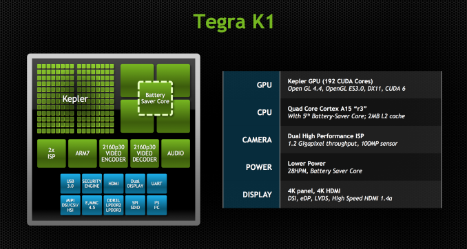
NVIDIA has taken to using CES as its platform for launching members of its Tegra mobile SoC family. This year was no different as it shifted branding a bit in its announcement of the Tegra K1, formerly known as Project Logan.
With Tegra 2 NVIDIA’s big selling point was being first to dual-core in Android. Tegra 3 attempted to do the same with being first to quad-core. Tegra 4 just made things faster. Tegra K1 on the other hand does away with the gimmicks and instead focuses on fundamentals.
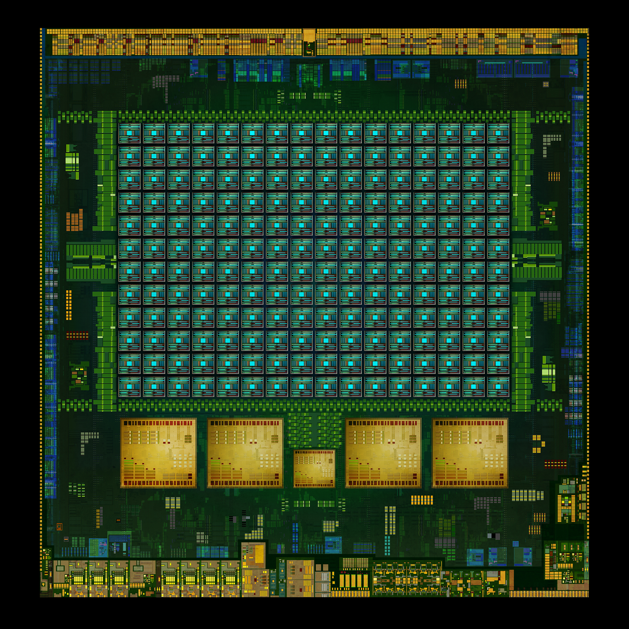
The SoC will come in two versions, one version with a quad-core (4+1) Cortex-A15, and one that leverages two of NVIDIA’s own 64-bit ARMv8 Denver CPUs. More importantly, they both ship with a full implementation of NVIDIA’s Kepler GPU architecture. In fact, Tegra K1 marks a substantial change in the way NVIDIA approaches mobile GPU design. From this point forward, all mobile GPUs will leverage the same architectures as NVIDIA’s desktop parts. As if that wasn’t enough, starting now, all future NVIDIA GeForce designs will begin first and foremost as mobile designs. NVIDIA just went from playing with mobile to dead serious in a heartbeat.
Tegra K1 will also be NVIDIA's launch vehicle for Project Denver, it's first fully custom ARMv8 CPU core. More on that in a bit.
CPU Option 1: Quad-Core ARM Cortex A15
Tegra K1 will ship in two configurations. The first went into production at the end of December 2013, is shipping to OEMs this quarter and will be in devices, allegedly, in the first half of 2014. This first configuration is based on ARM’s Cortex A15 CPU core.
Much like Tegra 4, the A15 version of Tegra K1 features four Cortex A15s synthesized for high frequencies and a fifth Cortex A15 that’s optimized for low power/frequency operation. The fifth core, what NVIDIA likes to call a shadow or companion core, is swapped in during periods of very low CPU usage (e.g. idle, screen off in your pocket updating new tweets/emails). As CPU demands grow the companion core is switched out for one of the four high performance cores, then two, then three and finally all four can be plugged in at once (but never five).
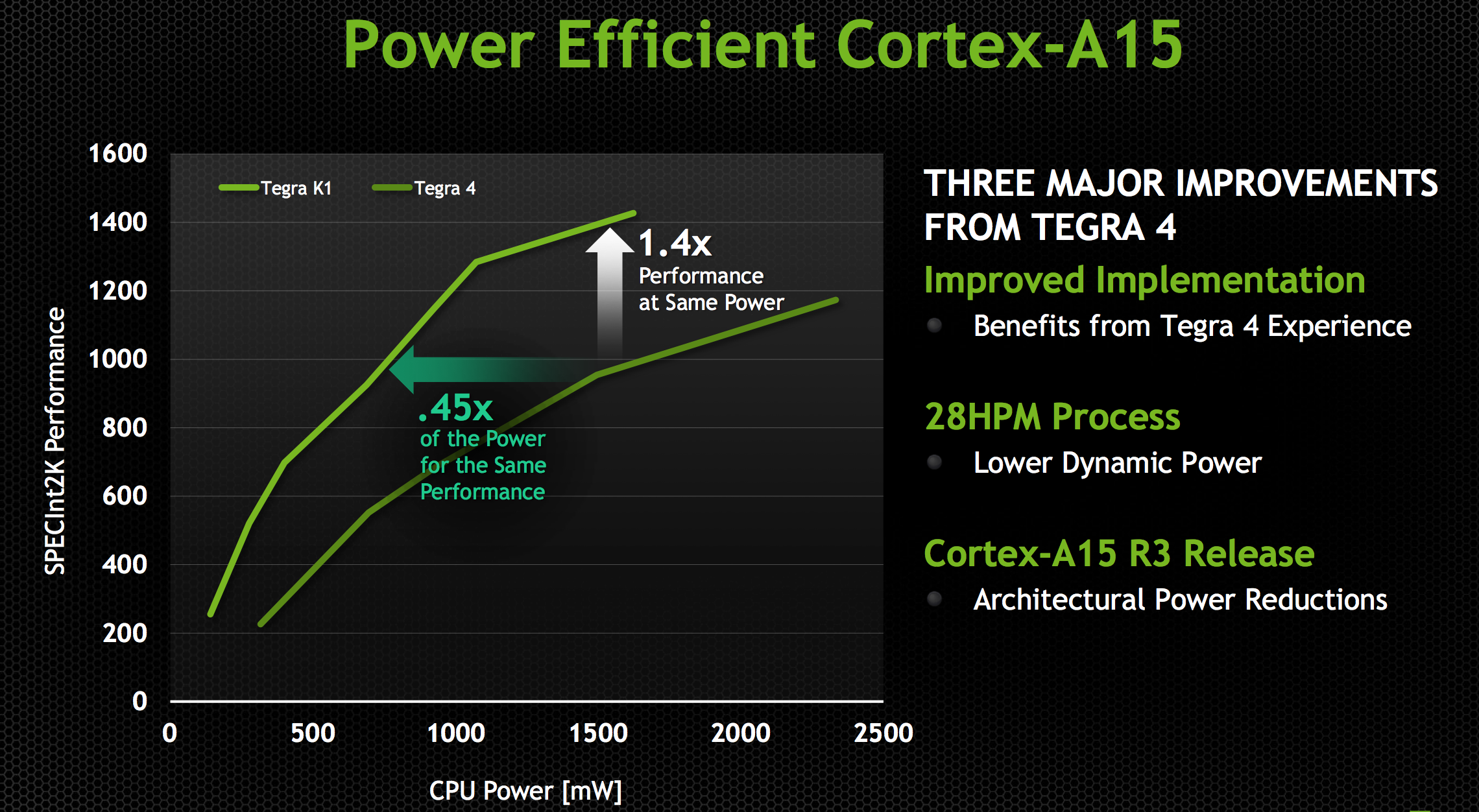
Tegra K1 ships with a newer revision of the Cortex A15 (r3p3) than what was in Tegra 4 (r2p1). ARM continuously updates its processor IP, with each revision bringing bug fixes and sometimes performance improvements. In the case of Tegra K1’s A15s, the main improvements here have to do with increasing power efficiency. With r3p0 (which r3p3 inherits) ARM added more fine grained clock gating, which should directly impact power efficiency.
The combination of the newer Cortex A15 revision and the move to 28nm HPM give Tegra K1 better performance at the same power consumption or lower power consumption at the same performance level. The reality tends to be that mobile OEMs will pursue max performance and not optimize for a good performance/power balance, but it’s at least possible to do better with Tegra K1 than with Tegra 4.
The max CPU clock goes up from 1.9GHz to 2.3GHz, a direct result of the move to 28nm HPM; 2.3GHz is the max CPU clock regardless of the number of active cores. The max performance increase over Tegra 4 running at max clocks will be just over 20%.
NVIDIA hasn’t made any changes to the L1/L2 cache configuration with Tegra K1. We’re still dealing with a shared 2MB L2 and 32KB/32KB L1s (I$+D$) per core.
The companion core can scale up to 1GHz, but tends to run at around 500MHz.
Feeding the CPU (and GPU) cores is a 64-bit wide LPDDR3 memory interface. NVIDIA will offer Tegra K1 in PoP, discrete and another package revision for standard clamshell notebook use.


88 Comments
View All Comments
name99 - Monday, January 6, 2014 - link
This is not especially new (though it might have been in Transmeta's time).Given the existence of robust and generally accurate branch prediction, a number of architectures have been proposed that are based on checkpoints and rollbacks rather than a ROB. There are a number of ways you can slice this, with the newest, richest, ideas having names like CFP (Continuous Flow Processing) and DOE (Distributed OutOfOrder Execution), both created by folks with Intel affiliations.
What these architectures do is help you with long memory latency delays because (in spite of what the above author said) OoO doesn't help much there. OoO covers L1 delays, most L2 delays, some L3 delays if you're lucky, and very little of the main memory delay. That's why prefetching is still an active area of research (e.g. there were some minor but cute improvements to prefetch in Ivy Bridge). The problem is the length of the ROB limits how far you can cover latency in a ROB architecture, and you can't make the ROB much larger because that increases the size (and slows down) the register file. Checkpoint architectures are not constrained in this way.
HOWEVER all this is neither here nor there.
There are three interesting claims being made about Denver
- it uses a checkpoint architecture. Interesting if true, because this type of architecture has the potential to be the general replacement for ROB OoO; even if the first implementation is only equivalent of ROB OoO, there are many new optimizations it opens up
- it uses some sort of "Code Morphing". Who knows WTF this means. Could be anything from rewriting ARM assembly to an internal ISA (like Apple have done many times, from 68K->PPC to Rosetta; likewise DEC did this to run x86 binaries on Alpha) to PPro style µOps to something very minor like the way POWER "cracks" a few instructions to simpler instructions.
- it is "7-wide". If this is an issue width, it's a bullshit measure that no-one who knows anything cares about. If this is a Decode/Rename/Dispatch width, it is a major leap forward, and the only likely way it is doable at such low power is through use of a trace cache which records dependency and remap information. If nVidia has this, it would be very cool.
Given that this is nVidia, my betting would be that every one of these is underwhelming. The exciting checkpoint architecture is in fact a standard ROB (with standard ROB limitations). The code morphing is minor cracking of a few "hard" instructions. The 7-wide refers to issue width so, ho-hum.
Loki726 - Tuesday, January 7, 2014 - link
"This is not especially new."Agreed. I mainly posted it for reference in case someone had not seen it before.
Da W - Monday, January 6, 2014 - link
For that matter i would prefer a Kabini surface mini and for AMD to follow Nvidia in game streaming (from PC or from Xbox one).chizow - Monday, January 6, 2014 - link
Great write-up guys, you're right, this is the most exciting announcement I've seen in the CPU/GPU/SoC space in a very long time, similar to A7 Cyclone but 2x that due to both CPU and GPU bombshells. It's probably the first analysis I've read in full because everything was just that interesting relative to what the rest of the industry is doing.One burning question that I did not see touched upon at all, here or elsewhere:
****What does Tegra K1 do for Nvidia's Kepler IP tech licensing prospects?
It seems to me, even if Tegra itself is not a smash hit for Nvidia in terms of design wins, the GPU technology is so disruptive that even if it gets into a few major designs (Surface 3, Nexus 7 2014, Asus Transformer for example) it may very well *FORCE* the other major industry players (Intel, Samsung, Apple) that don't have their own in-house graphics IP to license Kepler to remain competitive?
What do you all think? Any buzz on that front at CES?
OreoCookie - Friday, January 10, 2014 - link
As far as I can tell, nVidia only compared the GPU performance of the A7 to Tegra K1 but not the CPU performance. I'd be very curious to see how the Denver cores compare to Apple's Cyclone cores, though.Also, given Tegra's release date, it'll compete with Apple's A8.
Krysto - Saturday, January 11, 2014 - link
Based on the (limited) technical description and how massive those cores are, along with clock speeds that are almost twice as high as what Apple typically uses, I'd say they will beat Apple's A8 (probably just an upgraded Cyclone) pretty easily - unless Nvidia did something stupid with that software translation that adds too much overhead and and cuts the performance too much.But since we don't know exactly what's going on inside of those CPU cores, we'll have to wait for more details or a direct comparison (and hopefully Denver actually arrives this fall, and not next year).
OreoCookie - Sunday, January 12, 2014 - link
Initially, I thought so, too, but knowing it's a Transmeta Crusoe-like design, I'd be much more cautious about performance. At the same clockspeed, the Crusoe was about half or a third as fast as a Pentium III. The advantage was that the cpus consumed much less power.Of course that tells us nothing of a comparison between the A7 or A8 and a Denver-based K1 other than that the architectures are not directly comparable.
name99 - Monday, January 6, 2014 - link
"We’ve seen code morphing + binary translation done in the past, including famously in Transmeta’s offerings in the early 2000s, but it’s never been done all that well at the consumer client level.
"
Actually we've seen a few different versions of it which have worked just fine.
One obvious example (not consumer, but transparent) was IBM's switch over from custom cores to POWER cores for i-Series.
More on the consumer end, Apple have been doing this for years if you use OpenCL on their products --- they convert, on the fly, a byte code version of the GPU instructions to the target GPU. And of course anything that uses a JIT, whether it's targeting Java or JS (or Dalvik for that matter) is doing a similar sort of thing.
There may be uniquely painful aspects to doing this for x86/Windows, especially 15 years ago, but I don't think Transmeta's failure tells us anything --- this mainstream-ish tech. Especially now, in a world with hypervisors, where you have a more well-defined "space" for control code to run and bring up the OS step by step.
ruthan - Tuesday, January 7, 2014 - link
Ok, they maybe have enough GPU performance in this chip on paper. But how is final TDP SOC power consumation for 64 bit piece?But if you want to have realy PS3 or Xbox performance, which was advertised / promised till original Ipad and we still arent here at all.
Other problem are game engines middleware performance, because 80% of mobile games using Unity3D engine, which in by my experience, much more HW resources greedy and inefficient (C# - has automatic garbage collection, all in Unity running in single thread, GUI performance is terrible, PhysX implementation is signle thread) that, that console developement kits.
Back into problem, GPU is maybe ok, but for final overall performance you need also CPU with desktop like performance and to freed GPU with data and im dont think so that these weak ARM is nearly here.
So in overall i dont agree with these big perfromance and desktop like performance promises at all, would be ok, but it is only empty words.
kwrzesien - Tuesday, January 7, 2014 - link
I think nVidia has finally done it with a great SoC/GPU! I hope they get a few very solid design wins, it could change alot.Looking at those beautiful chip diagrams I think they have the CPU/CPU balance just right.