The Haswell Review: Intel Core i7-4770K & i5-4670K Tested
by Anand Lal Shimpi on June 1, 2013 10:00 AM ESTDie Size and Transistor Count
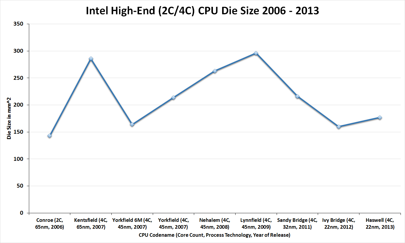
Moving on to die sizes and transistor counts, this year Intel is striving to be more straightforward and accurate than was the case with Sandy Bridge and Ivy Bridge. With the Bridge generation we didn’t initially get comparable numbers, only for the correction to throw in additional confusion. For Haswell Intel is laying things out from the start, listing both possible numbers so that either can be compared.
| CPU Specification Comparison | |||||||||
| CPU | Manufacturing Process | Cores | GPU | Transistor Count (Schematic) | Die Size | ||||
| Haswell GT3 4C | 22nm | 4 | GT3 | ? | 264mm2 (est) | ||||
| Haswell GT2 4C | 22nm | 4 | GT2 | 1.4B | 177mm2 | ||||
| Haswell ULT GT3 2C | 22nm | 2 | GT3 | 1.3B | 181mm2 | ||||
| Intel Ivy Bridge 4C | 22nm | 4 | GT2 | 1.2B | 160mm2 | ||||
| Intel Sandy Bridge E 6C | 32nm | 6 | N/A | 2.27B | 435mm2 | ||||
| Intel Sandy Bridge 4C | 32nm | 4 | GT2 | 995M | 216mm2 | ||||
| Intel Lynnfield 4C | 45nm | 4 | N/A | 774M | 296mm2 | ||||
| AMD Trinity 4C | 32nm | 4 | 7660D | 1.303B | 246mm2 | ||||
| AMD Vishera 8C | 32nm | 8 | N/A | 1.2B | 315mm2 | ||||
The two numbers for the most common Haswell configuration, Haswell GT2 4C, are 1.4 billion schematic transistors and 1.6 billion layout transistors. Why and what is the difference? The former count is the number of transistors in the schematic (hence the name), and is generally the number we go by when quoting transistor counts. Meanwhile the second number, the layout number, is the number of transistors used in the fabrication process itself. The difference comes from the fact that while the schematic will use one large transistor – being a logical diagram – production will actually use multiple transistors laid out in parallel for layout and process reasons. So how many transistors does Haswell have? It has both 1.4B and 1.6B, depending on which number we’re after, with 1.4B being the number Intel is passing around.
In any case, even among quad cores Haswell is going to come in a couple of different sizes. Along with the 1.4B transistor, 177mm2 4C/GT2 version of Haswell, there is the 4C/GT3 version of Haswell, which Intel doesn’t list the die size or transistor count for. Based on our rough measurements of the physical die we’re at 264mm2, which including the epoxy covering the die will run a bit large.
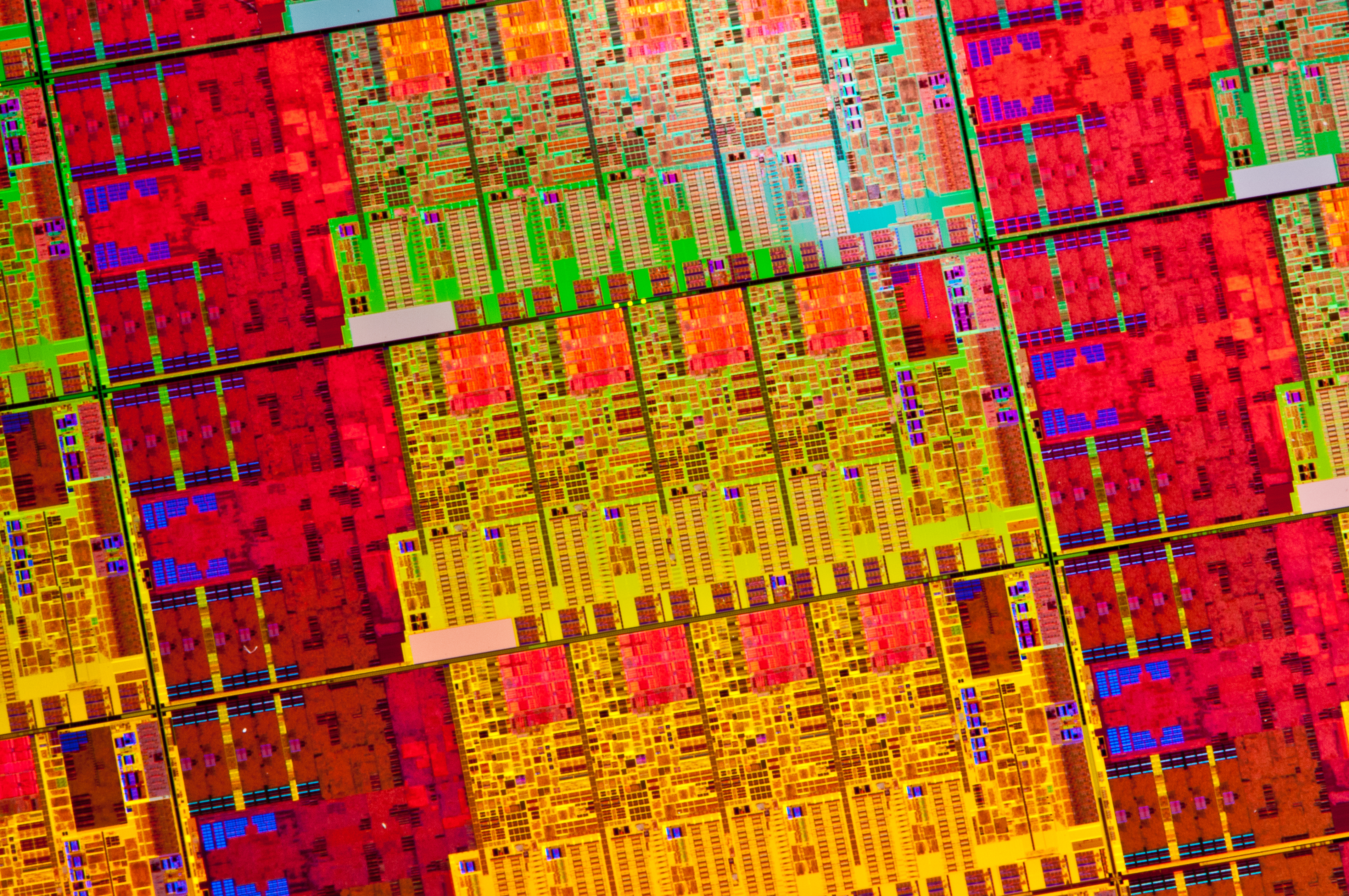
Breaking things down to the GPU portion of Haswell, based in turn on these measurements I came up with an 87mm^2 adder for the extra hardware in Haswell GT3 vs. GT2. Doubling that 87mm^2 we get a rough idea of how big the full 40 EU Haswell GPU might be: 174mm^2. If my math is right, this means that in a quad-core Haswell GT3 die, around 65% of the die area is GPU. This is contrary to the ~33% in a quad-core Haswell GT2. I suspect a dual-core + GT3 design is at least half GPU. Meanwhile Crystalwell, the 128MB eDRAM, adds another 84mm2 die (by our measurements) to the entire package.
On a comparative basis, the 4C/GT2 version of Haswell is roughly 200M transistors and 17mm2 bigger than the comparable 4C/GT2 version of Ivy Bridge. The transistor count increase is roughly what we’d expect, with most of those transistors going to Haswell itself while the GPU remains relatively unchanged. Though it’s interesting to note that while this marks a 17% increase in transistors, it’s only an 11% increase in die size. Ivy Bridge was a small die for an Intel, and while Haswell grows larger in exchange for the additional functionality the new architecture provides, it’s still a fairly small GPU and reaches a density greater than Ivy Bridge itself. Or to put this another way, Intel’s last tock CPU, Sandy Bridge, was larger still by almost 40mm2. It’s only once we start adding the relatively big GT3 GPU, and not the CPU, that we see Intel go well above 200mm2.


210 Comments
View All Comments
Nacho - Saturday, June 1, 2013 - link
Maybe it's time to upgrade my C2D E4300? :Pkrumme - Saturday, June 1, 2013 - link
Absolutely, go get a good ssd and this processor or IB, if its for desktop.Oscarcharliezulu - Monday, June 3, 2013 - link
Do it.Boissez - Saturday, June 1, 2013 - link
So my 2½ year old 2600K ($317) performs about the same as todays 4560K ($242). Color me underwhelmed.Meanwhile in mobileland we've went from 1 Ghz Tegra 2 to 2 Ghz Snapdragon S600 within the same timespan.
tential - Saturday, June 1, 2013 - link
Because for 99.9% of the population what's out there today is more than fast enough. Hell, the Core2Duo Conroe/Penryn processors are fast enough for most people today. I'm still using one in fact.On the mobile side however, we have tons of applications that could use more power. My galaxy S3 takes a little to load up some games, and while the data may have been downloaded to the phone through wifi, it still isn't on my screen yet.
I think it's pretty obvious why you see mobile land having to progress so fast while desktop processors are focusing on power consumption as the AVERAGE consumer (not people who are techies) would prefer smaller PCs and pushing more power efficient processors into smaller and smaller things like the intel NUC is what the consumer desires.
In short:
Your desires are the 1%. The 99% are being catered to.
klmccaughey - Monday, June 3, 2013 - link
@tential: Your last statement, maybe it should read "OUR desires are the 1%"? ;) I bet we would all be clapping right now if the 4770k was a big upgrade. Well, most of us, I think?jeffkibuule - Saturday, June 1, 2013 - link
Mobile is having the same performance renaissance that desktop chips had from 2004-2006 when we went from a hot, bloated Pentium 4 to a cool, efficient Core 2 Duo. And certainly we've had performance gains since then, but eventually the gains won't come so easily. You can start to see that a bit now with how the Exynos 5250 in the Nexus 10 is thermally throttled to 4W such that CPU and GPU can't be both running full tilt at the same time.Homeles - Saturday, June 1, 2013 - link
You're disappointed because your understanding of physics and Moore's Law is poorly developed. The scenario you've provided is a blatant false equivalency.According to your desperate desires, the roughly 4GHz processors that launched with Sandy Bridge should be running at twice the clock speed today.
When you understand that leakage power grows exponentially as transistor geometries shrink, and that power consumption raises exponentially as clock speed rises, you will realize that even the 10% gains that Haswell makes here are a big deal.
Dal Makhani - Saturday, June 1, 2013 - link
Homeles, I really appreciate your well said comment, im taking a business degree with an accounting major, but ive always loved building PC's as a hobby. When some of my computer science/engineer friends try to show me the stuff they are learning, i am baffled as its not my area of expertise. I can only imagine how challenging it is to combat the shrinking processes and make performance gains as you said. I have deep respect for Intel and AMD, always trying to utilize their research and engineers to try and make any gains for society. These forum people are just so ignorant sometimes and it baffles me.chizow - Saturday, June 1, 2013 - link
Hey, similar path as me. :) Don't worry about lack of understanding now, stick to it, keep reading great technical sites like AT, keep an open mind, and you'll get a really good grip on the industry, especially if you are an actual user/enthusiast of the products.