The Haswell Review: Intel Core i7-4770K & i5-4670K Tested
by Anand Lal Shimpi on June 1, 2013 10:00 AM ESTDie Size and Transistor Count
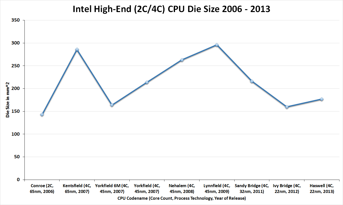
Moving on to die sizes and transistor counts, this year Intel is striving to be more straightforward and accurate than was the case with Sandy Bridge and Ivy Bridge. With the Bridge generation we didn’t initially get comparable numbers, only for the correction to throw in additional confusion. For Haswell Intel is laying things out from the start, listing both possible numbers so that either can be compared.
| CPU Specification Comparison | |||||||||
| CPU | Manufacturing Process | Cores | GPU | Transistor Count (Schematic) | Die Size | ||||
| Haswell GT3 4C | 22nm | 4 | GT3 | ? | 264mm2 (est) | ||||
| Haswell GT2 4C | 22nm | 4 | GT2 | 1.4B | 177mm2 | ||||
| Haswell ULT GT3 2C | 22nm | 2 | GT3 | 1.3B | 181mm2 | ||||
| Intel Ivy Bridge 4C | 22nm | 4 | GT2 | 1.2B | 160mm2 | ||||
| Intel Sandy Bridge E 6C | 32nm | 6 | N/A | 2.27B | 435mm2 | ||||
| Intel Sandy Bridge 4C | 32nm | 4 | GT2 | 995M | 216mm2 | ||||
| Intel Lynnfield 4C | 45nm | 4 | N/A | 774M | 296mm2 | ||||
| AMD Trinity 4C | 32nm | 4 | 7660D | 1.303B | 246mm2 | ||||
| AMD Vishera 8C | 32nm | 8 | N/A | 1.2B | 315mm2 | ||||
The two numbers for the most common Haswell configuration, Haswell GT2 4C, are 1.4 billion schematic transistors and 1.6 billion layout transistors. Why and what is the difference? The former count is the number of transistors in the schematic (hence the name), and is generally the number we go by when quoting transistor counts. Meanwhile the second number, the layout number, is the number of transistors used in the fabrication process itself. The difference comes from the fact that while the schematic will use one large transistor – being a logical diagram – production will actually use multiple transistors laid out in parallel for layout and process reasons. So how many transistors does Haswell have? It has both 1.4B and 1.6B, depending on which number we’re after, with 1.4B being the number Intel is passing around.
In any case, even among quad cores Haswell is going to come in a couple of different sizes. Along with the 1.4B transistor, 177mm2 4C/GT2 version of Haswell, there is the 4C/GT3 version of Haswell, which Intel doesn’t list the die size or transistor count for. Based on our rough measurements of the physical die we’re at 264mm2, which including the epoxy covering the die will run a bit large.
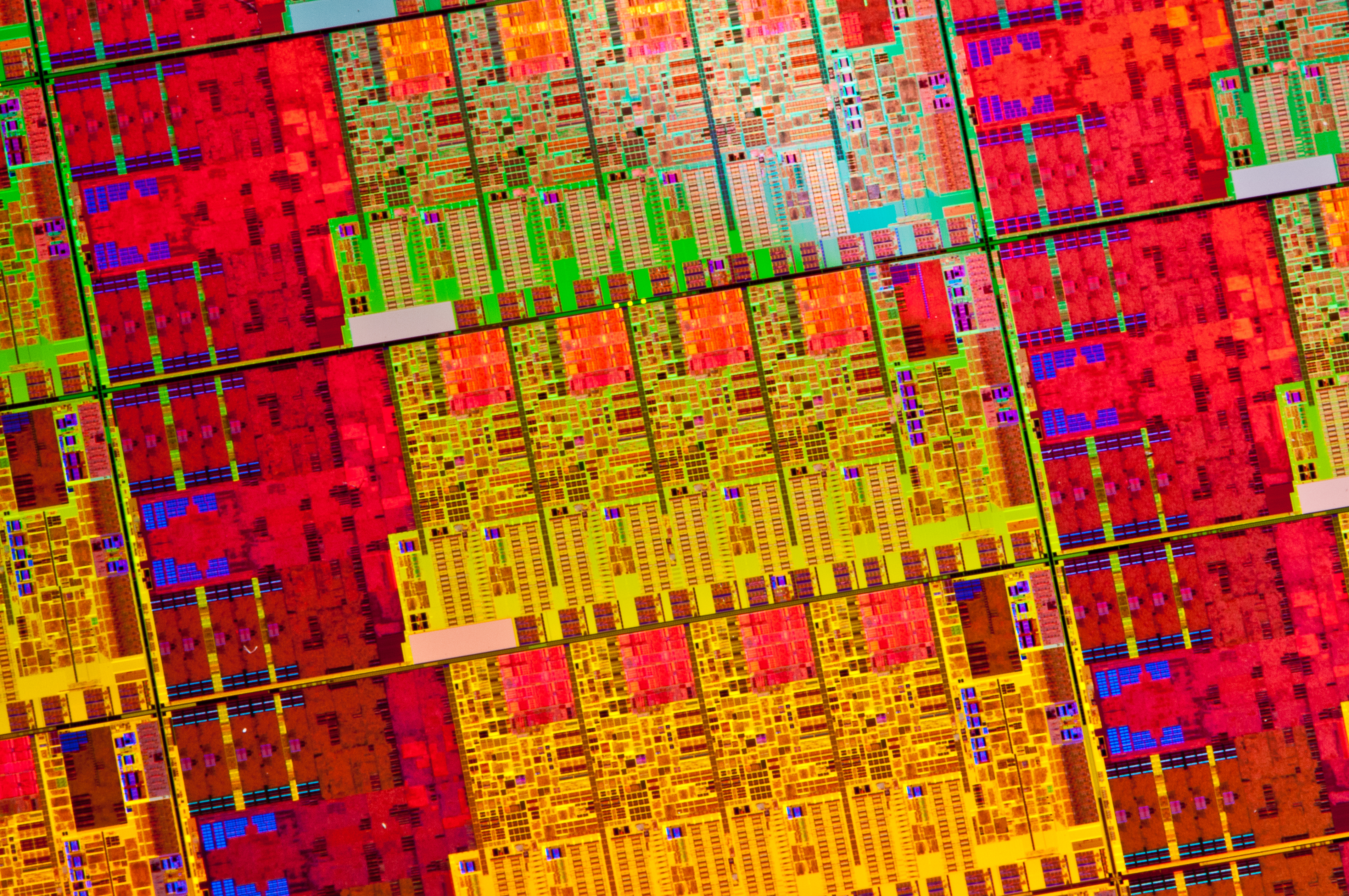
Breaking things down to the GPU portion of Haswell, based in turn on these measurements I came up with an 87mm^2 adder for the extra hardware in Haswell GT3 vs. GT2. Doubling that 87mm^2 we get a rough idea of how big the full 40 EU Haswell GPU might be: 174mm^2. If my math is right, this means that in a quad-core Haswell GT3 die, around 65% of the die area is GPU. This is contrary to the ~33% in a quad-core Haswell GT2. I suspect a dual-core + GT3 design is at least half GPU. Meanwhile Crystalwell, the 128MB eDRAM, adds another 84mm2 die (by our measurements) to the entire package.
On a comparative basis, the 4C/GT2 version of Haswell is roughly 200M transistors and 17mm2 bigger than the comparable 4C/GT2 version of Ivy Bridge. The transistor count increase is roughly what we’d expect, with most of those transistors going to Haswell itself while the GPU remains relatively unchanged. Though it’s interesting to note that while this marks a 17% increase in transistors, it’s only an 11% increase in die size. Ivy Bridge was a small die for an Intel, and while Haswell grows larger in exchange for the additional functionality the new architecture provides, it’s still a fairly small GPU and reaches a density greater than Ivy Bridge itself. Or to put this another way, Intel’s last tock CPU, Sandy Bridge, was larger still by almost 40mm2. It’s only once we start adding the relatively big GT3 GPU, and not the CPU, that we see Intel go well above 200mm2.


210 Comments
View All Comments
Khato - Sunday, June 2, 2013 - link
Based on the published Haswell 4C GT2 die shot I believe that your estimates for the graphics area are quite high. It's relatively simple to derive the graphics area on 4C GT2 now that we know the total die size - should be somewhere in the vicinity of 58mm^2. Double that and you get 116mm^2 for GT3.As for the remaining 29mm^2 delta between 4C GT2 and 4C GT3 die sizes... I'd chalk that up to both inefficiencies due to going with a more square die instead of the long and skinny that's been with us since SNB and the extra logic/IOs necessary for the eDRAM L4.
Regardless, there's no question that the 174mm^2 figure for GT3 is incorrect as the 4 cores, associated L3, and system agent on the 4C GT2 die take up approximately 119mm^2, and adding 174mm^2 to that would yield a 293mm^2 die size.
Bobsama - Sunday, June 2, 2013 - link
I too am on a Core i7-950. I bought it in April 2012. If this system died and I was building anew, I'd probably do it--I'd probably grab an i7-4770K. But for $500, notta chance!LeetMiniWheat - Sunday, June 2, 2013 - link
Would have been nice to see some actual CPU-bound games, like Skyrim. Or something low res to take the load completely off the GPU.roltzje - Sunday, June 2, 2013 - link
It doesn't take a genius to figure whats going on here. Competition spurs innovation. There is no competition for mid-high end desktop processors, or even laptop processors really. AMD only keeps up with mid range because they have to set very high clocks on their inferior architecture.Where the competition is is in mobile. Smartphones and tablets. By moving Haswell down this generation, Intel is getting themselves closer to be a true competitor in that space. This year we should see a power and battery life combination that ARM cannot reach.
There are also huge gains for gaming and gaming laptops. A 14-15" mid-ranger cost $500 with Iris graphics should be able to run most games decently now without all-minimum settings. Especially given that the PS4 and XBO are running x86 low to mid range graphics, I can easily see Haswell notebooks keeping up, especially Iris pro laptops, which I would assume can come in under $1000 and in relatively slim form factors.
deepblue08 - Sunday, June 2, 2013 - link
I think they should benchmarks this new CPU with 2-3GPUs. I don't think 1 video card is enough to really test the strength of new cpus, which is why the difference between ivy bridge and haswell is so small. Give them 2-3 GPUs to work with and see if they can really step-up.Yahma - Sunday, June 2, 2013 - link
YAWN... with no competition from AMD, Haswell offers none to just a few % improvement over the previous generation (depending on who's benchmarks you believe), higher power consumption, and fewer features (ie. no virtualization extensions on the higher end models) all at a higher price that requires one to purchase a new motherboard.... No Thanks!just4U - Sunday, June 2, 2013 - link
That was covered in a previous article.. it was established that the 3770K was the go to cpu for multiple video card systems. (altho.. I'd say this would do in a pinch as would the previous 2600/2700K)Yahma - Sunday, June 2, 2013 - link
YAWN... with no competition from AMD, Haswell offers none to just a few % improvement over the previous generation (depending on who's benchmarks you believe), higher power consumption, and fewer features (ie. no virtualization extensions on the higher end models) all at a higher price that requires one to purchase a new motherboard.... No Thanks!mcbowler - Sunday, June 2, 2013 - link
thanks for posting "CPU Performance: Going Even Further Back" almost twice as fast as my i5 750. I just might upgrade when the NCASE M1 is available.araczynski - Sunday, June 2, 2013 - link
either way, should be a serious boost in power to my aging E8500 :)