The Haswell Review: Intel Core i7-4770K & i5-4670K Tested
by Anand Lal Shimpi on June 1, 2013 10:00 AM ESTDie Size and Transistor Count
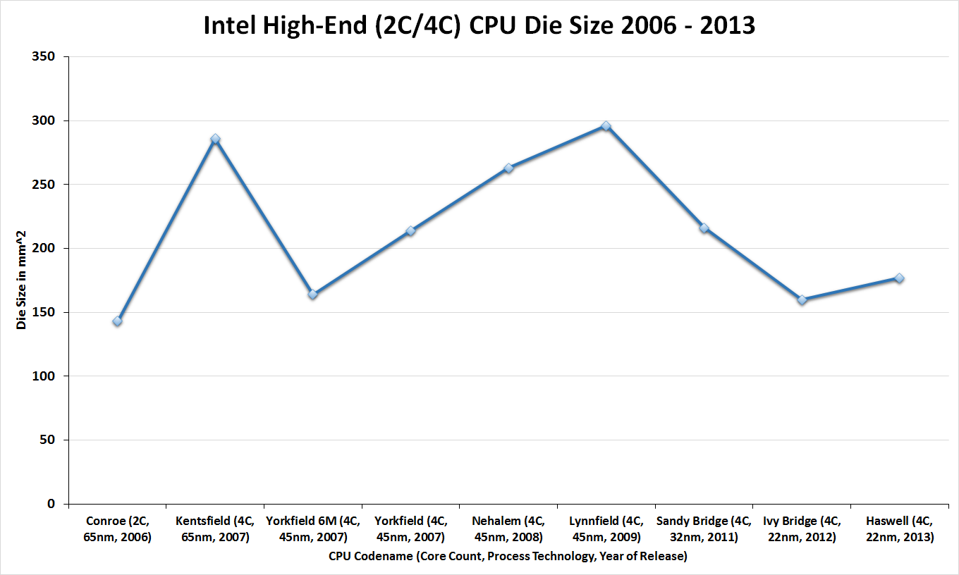
Moving on to die sizes and transistor counts, this year Intel is striving to be more straightforward and accurate than was the case with Sandy Bridge and Ivy Bridge. With the Bridge generation we didn’t initially get comparable numbers, only for the correction to throw in additional confusion. For Haswell Intel is laying things out from the start, listing both possible numbers so that either can be compared.
| CPU Specification Comparison | |||||||||
| CPU | Manufacturing Process | Cores | GPU | Transistor Count (Schematic) | Die Size | ||||
| Haswell GT3 4C | 22nm | 4 | GT3 | ? | 264mm2 (est) | ||||
| Haswell GT2 4C | 22nm | 4 | GT2 | 1.4B | 177mm2 | ||||
| Haswell ULT GT3 2C | 22nm | 2 | GT3 | 1.3B | 181mm2 | ||||
| Intel Ivy Bridge 4C | 22nm | 4 | GT2 | 1.2B | 160mm2 | ||||
| Intel Sandy Bridge E 6C | 32nm | 6 | N/A | 2.27B | 435mm2 | ||||
| Intel Sandy Bridge 4C | 32nm | 4 | GT2 | 995M | 216mm2 | ||||
| Intel Lynnfield 4C | 45nm | 4 | N/A | 774M | 296mm2 | ||||
| AMD Trinity 4C | 32nm | 4 | 7660D | 1.303B | 246mm2 | ||||
| AMD Vishera 8C | 32nm | 8 | N/A | 1.2B | 315mm2 | ||||
The two numbers for the most common Haswell configuration, Haswell GT2 4C, are 1.4 billion schematic transistors and 1.6 billion layout transistors. Why and what is the difference? The former count is the number of transistors in the schematic (hence the name), and is generally the number we go by when quoting transistor counts. Meanwhile the second number, the layout number, is the number of transistors used in the fabrication process itself. The difference comes from the fact that while the schematic will use one large transistor – being a logical diagram – production will actually use multiple transistors laid out in parallel for layout and process reasons. So how many transistors does Haswell have? It has both 1.4B and 1.6B, depending on which number we’re after, with 1.4B being the number Intel is passing around.
In any case, even among quad cores Haswell is going to come in a couple of different sizes. Along with the 1.4B transistor, 177mm2 4C/GT2 version of Haswell, there is the 4C/GT3 version of Haswell, which Intel doesn’t list the die size or transistor count for. Based on our rough measurements of the physical die we’re at 264mm2, which including the epoxy covering the die will run a bit large.
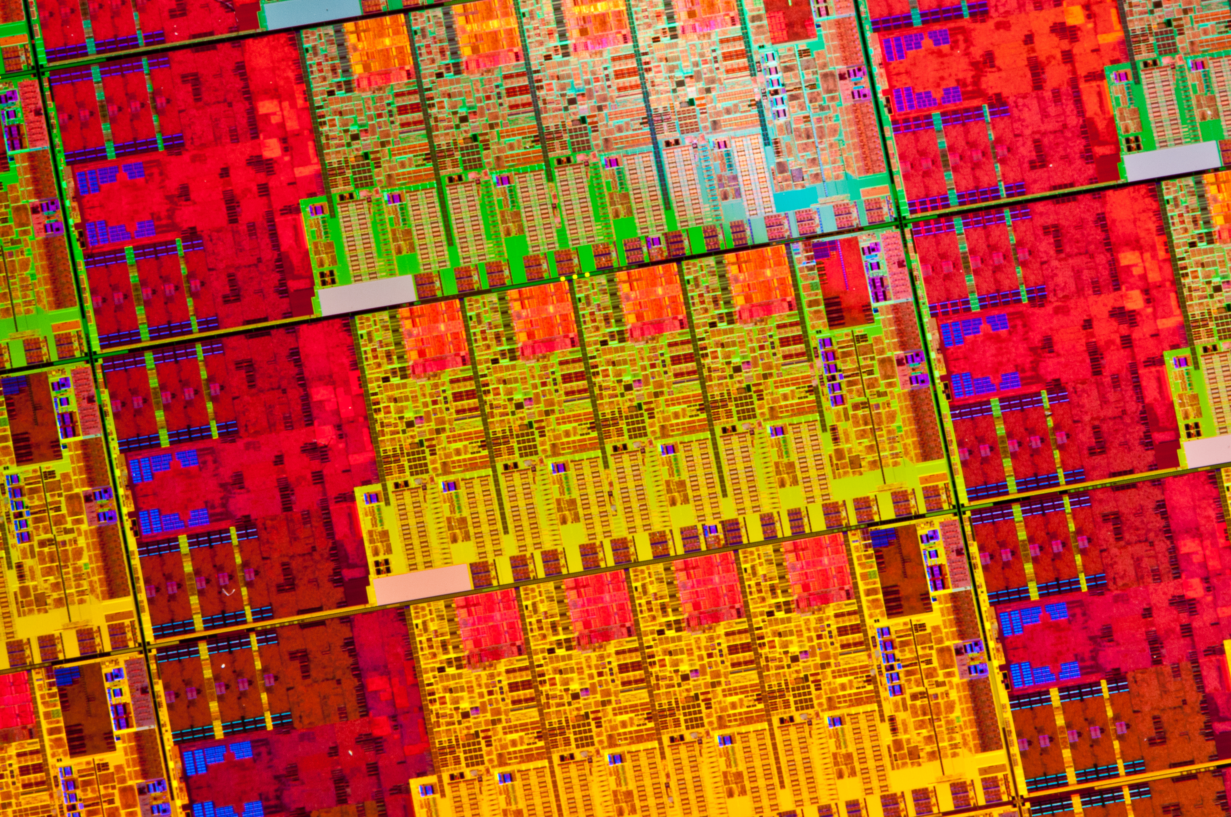
Breaking things down to the GPU portion of Haswell, based in turn on these measurements I came up with an 87mm^2 adder for the extra hardware in Haswell GT3 vs. GT2. Doubling that 87mm^2 we get a rough idea of how big the full 40 EU Haswell GPU might be: 174mm^2. If my math is right, this means that in a quad-core Haswell GT3 die, around 65% of the die area is GPU. This is contrary to the ~33% in a quad-core Haswell GT2. I suspect a dual-core + GT3 design is at least half GPU. Meanwhile Crystalwell, the 128MB eDRAM, adds another 84mm2 die (by our measurements) to the entire package.
On a comparative basis, the 4C/GT2 version of Haswell is roughly 200M transistors and 17mm2 bigger than the comparable 4C/GT2 version of Ivy Bridge. The transistor count increase is roughly what we’d expect, with most of those transistors going to Haswell itself while the GPU remains relatively unchanged. Though it’s interesting to note that while this marks a 17% increase in transistors, it’s only an 11% increase in die size. Ivy Bridge was a small die for an Intel, and while Haswell grows larger in exchange for the additional functionality the new architecture provides, it’s still a fairly small GPU and reaches a density greater than Ivy Bridge itself. Or to put this another way, Intel’s last tock CPU, Sandy Bridge, was larger still by almost 40mm2. It’s only once we start adding the relatively big GT3 GPU, and not the CPU, that we see Intel go well above 200mm2.


210 Comments
View All Comments
jmcb - Saturday, June 1, 2013 - link
I currently have an E8400 so the Haswell would be amazing....but I will go for amazing and value._zenith - Saturday, June 1, 2013 - link
"Even on the dekstop" - desktop. Just spelling gripe.I notice the gains over Nehalem are pretty much the same that you can *easily* get (just increase VCore and BCLK) out of overclocking Nehalem. So now they're neck and neck if you don't overclock the Haswell part. Maybe my system will be good for another year now! (i7-920 @ 4.0).
Da W - Saturday, June 1, 2013 - link
YeehaaaNow i can buy my Trinity + Radeon rig for the price of a haswell only rig. I know it will play every videogame made for xbox or PS4 for the next 7-8 years and make a perfect HTPC!
ChefJeff789 - Saturday, June 1, 2013 - link
I've been sitting on a first-gen Core i7 and this is still a little dissapointing. It is significantly quicker than mine, but I'm not sure that the upgrade is quite worth it for me yet as everything I use runs reasonably well. I am interested in the new socket type, though. I wonder if upgrading the motherboard with a decent Haswell would benefit me later on with a Skylake. It's hard to say; I haven't seen any firm specs on the socket-type for the Skylake chips.jwcalla - Saturday, June 1, 2013 - link
At this point I think there are more interesting places to put your tech dollars. A high-DPI display or triple monitors if you're into gaming, more SSDs if you need the space, a NAS or a nice tablet, etc. I'm in your camp with an i7-870 and nothing I do pushes it enough to test my patience.kyuu - Saturday, June 1, 2013 - link
Agreed -- unless you're loaded, there are far more interesting ways to spend your money in the PC arena than on the overhyped and underwhelming Haswell SKUs. Unless you're still stuck on Phenom II or Core2Duo.bji - Sunday, June 2, 2013 - link
Hey - I'm still "stuck" on a Phenom II (in my desktop; laptop is 15 inch rMBP with Ivy Bridge) and it's not that bad. It's significantly slower than the Bridges in single threaded apps but even so it's fast enough that I never notice, much like jwcalla never notices with his i7-870. And the Phenom II x6 has 6 real cores that do decently well in heavily multithreaded apps, really extensive compiles being the only thing that I ever do that would benefit at all from extra speed. 6 real cores holding their own reasonably well there. Even if an Ivy Bridge were 50% faster per core on the compiles (and it probably is), the x6 has 50% more cores so it kind of evens out ...rabbatabba - Sunday, June 2, 2013 - link
Anyone know if x264 is properly optimized for AVX2? Naiively, one might expect a 2x speedup for SIMD integer dominated code over the AVX1-only 2700k provided that the rest of the system is able to shuffle around data.http://com3.tv/wp-content/uploads/2012/09/Haswell-...
I am very curious as to the real-world performance gains of integer (and floating-point FMA) SIMD code in Haswell compared to previous generations.
Klimax - Sunday, June 2, 2013 - link
It has support for AVX2. Not sure in how many places, but over months there was stream of AVX2 code paths.plopingo - Sunday, June 2, 2013 - link
No need for me to upgrade with my I7 960@4.2ghzmaybe next time :D