The Haswell Review: Intel Core i7-4770K & i5-4670K Tested
by Anand Lal Shimpi on June 1, 2013 10:00 AM ESTDie Size and Transistor Count
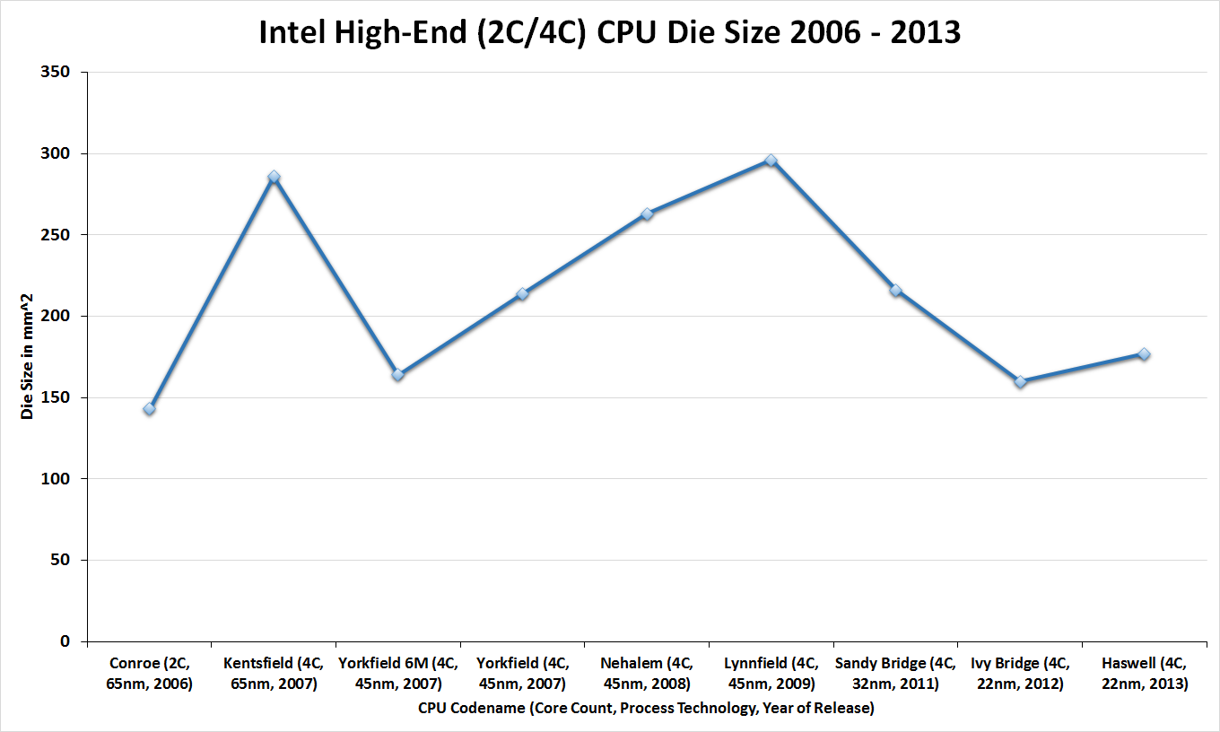
Moving on to die sizes and transistor counts, this year Intel is striving to be more straightforward and accurate than was the case with Sandy Bridge and Ivy Bridge. With the Bridge generation we didn’t initially get comparable numbers, only for the correction to throw in additional confusion. For Haswell Intel is laying things out from the start, listing both possible numbers so that either can be compared.
| CPU Specification Comparison | |||||||||
| CPU | Manufacturing Process | Cores | GPU | Transistor Count (Schematic) | Die Size | ||||
| Haswell GT3 4C | 22nm | 4 | GT3 | ? | 264mm2 (est) | ||||
| Haswell GT2 4C | 22nm | 4 | GT2 | 1.4B | 177mm2 | ||||
| Haswell ULT GT3 2C | 22nm | 2 | GT3 | 1.3B | 181mm2 | ||||
| Intel Ivy Bridge 4C | 22nm | 4 | GT2 | 1.2B | 160mm2 | ||||
| Intel Sandy Bridge E 6C | 32nm | 6 | N/A | 2.27B | 435mm2 | ||||
| Intel Sandy Bridge 4C | 32nm | 4 | GT2 | 995M | 216mm2 | ||||
| Intel Lynnfield 4C | 45nm | 4 | N/A | 774M | 296mm2 | ||||
| AMD Trinity 4C | 32nm | 4 | 7660D | 1.303B | 246mm2 | ||||
| AMD Vishera 8C | 32nm | 8 | N/A | 1.2B | 315mm2 | ||||
The two numbers for the most common Haswell configuration, Haswell GT2 4C, are 1.4 billion schematic transistors and 1.6 billion layout transistors. Why and what is the difference? The former count is the number of transistors in the schematic (hence the name), and is generally the number we go by when quoting transistor counts. Meanwhile the second number, the layout number, is the number of transistors used in the fabrication process itself. The difference comes from the fact that while the schematic will use one large transistor – being a logical diagram – production will actually use multiple transistors laid out in parallel for layout and process reasons. So how many transistors does Haswell have? It has both 1.4B and 1.6B, depending on which number we’re after, with 1.4B being the number Intel is passing around.
In any case, even among quad cores Haswell is going to come in a couple of different sizes. Along with the 1.4B transistor, 177mm2 4C/GT2 version of Haswell, there is the 4C/GT3 version of Haswell, which Intel doesn’t list the die size or transistor count for. Based on our rough measurements of the physical die we’re at 264mm2, which including the epoxy covering the die will run a bit large.
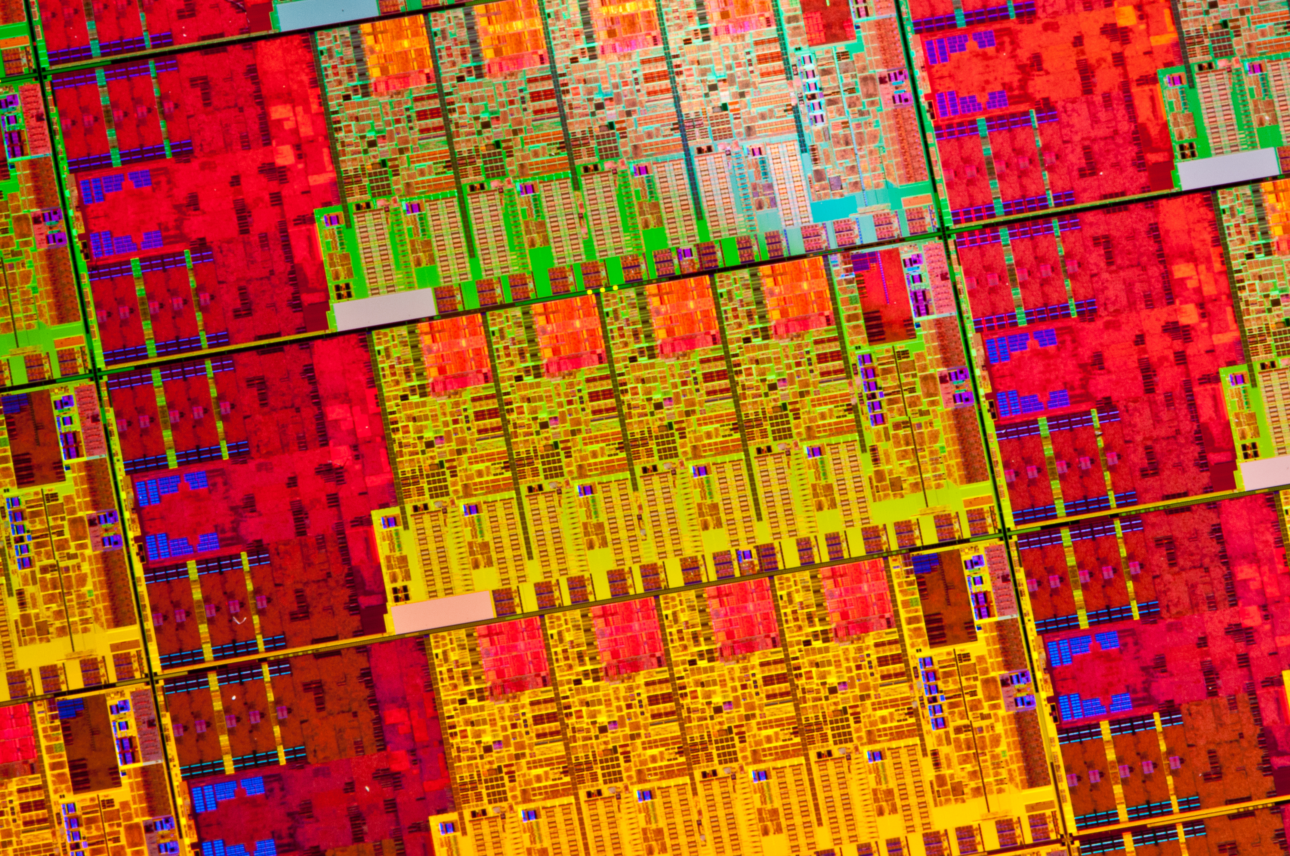
Breaking things down to the GPU portion of Haswell, based in turn on these measurements I came up with an 87mm^2 adder for the extra hardware in Haswell GT3 vs. GT2. Doubling that 87mm^2 we get a rough idea of how big the full 40 EU Haswell GPU might be: 174mm^2. If my math is right, this means that in a quad-core Haswell GT3 die, around 65% of the die area is GPU. This is contrary to the ~33% in a quad-core Haswell GT2. I suspect a dual-core + GT3 design is at least half GPU. Meanwhile Crystalwell, the 128MB eDRAM, adds another 84mm2 die (by our measurements) to the entire package.
On a comparative basis, the 4C/GT2 version of Haswell is roughly 200M transistors and 17mm2 bigger than the comparable 4C/GT2 version of Ivy Bridge. The transistor count increase is roughly what we’d expect, with most of those transistors going to Haswell itself while the GPU remains relatively unchanged. Though it’s interesting to note that while this marks a 17% increase in transistors, it’s only an 11% increase in die size. Ivy Bridge was a small die for an Intel, and while Haswell grows larger in exchange for the additional functionality the new architecture provides, it’s still a fairly small GPU and reaches a density greater than Ivy Bridge itself. Or to put this another way, Intel’s last tock CPU, Sandy Bridge, was larger still by almost 40mm2. It’s only once we start adding the relatively big GT3 GPU, and not the CPU, that we see Intel go well above 200mm2.


210 Comments
View All Comments
chizow - Saturday, June 1, 2013 - link
The other big problem with the CPU space besides the problems with power consumption and frequency, is the fact Intel has stopped using it's extra transistor budget from a new process node on the actual CPU portion of the die long ago. Most of the increased transistor budget afforded by a new process goes right to the GPU. We will probably not see a stop to this for some time until Intel reaches discrete performance equivalency.Jaybus - Monday, June 3, 2013 - link
Well, I don't know. Cache sizes have increased dramatically.chizow - Monday, June 3, 2013 - link
Not per core, these parts are still 4C 8MB, same as my Nehalem-based i7. Some of the SB-E boards have more cache per core, 4C 10MB on the 3820, 6C 15MB on the 3960/3970, but the extra bit results in a negligible difference over the 2MB per core on the 3930K.Boissez - Sunday, June 2, 2013 - link
I think you've misunderstood me.I'm merely pointing out that, in the past 2½ years we've barely seen any performance improvements in the 250-300$ market from Intel. And that is in stark contrast to the developments in mobileland. They too, are bound by the constraints you mention.
And please, stop the pompous know-it-all attitude. For the record, power consumption actually rises *linearly* with clock speed and *quadratically* with voltage. If your understanding of Joule's law and Ohm's law where better developed you would know.
klmccaughey - Monday, June 3, 2013 - link
Exactly. And it won't change until we see optical/biological chips or some other such future-tech breakthrough. As it is the electrons are starting to behave in light/waveform fashion at higher frequencies if I remember correctly from my semiconductor classes (of some years ago I might add).Jaybus - Monday, June 3, 2013 - link
Yes, but we will first see hybrid approaches. Intel, IBM, and others have been working on them and are getting close. Sure, optical interconnects have been available for some time, but not as an integrated on-chip feature which is now being called "silicon photonics". Many of the components are already there; micro-scale lenses, waveguides, and other optical components, avalanche photodiode detectors able to detect a very tiny photon flux, etc. All of those can be crafted with existing CMOS processes. The missing link is a cheaply made micro-scale laser.Think about it. An on-chip optical transceiver at THz frequencies allows optical chip-to-chip data transfer at on-chip electronic bus speeds, or faster. There is no need for L2 or L3 cache. Multiple small dies can be linked together to form a larger virtual die, increasing productivity and reducing cost. What if you could replace a 256 trace memory bus on a GPU with a single optical signal? There are huge implications both for performance and power use, even long before there are photonic transistors. Don't know about biological, but optical integration could make a difference in the not-so-far-off future.
tipoo - Saturday, June 1, 2013 - link
It's easier to move upwards from where ARM chips started a few years back. A bit like a developing economy showing growth numbers you would never see in a developed one.Genx87 - Saturday, June 1, 2013 - link
Interesting review. But finding it hard to justify replacing my i2500K. I guess next summer on the next iteration?kyuu - Saturday, June 1, 2013 - link
Agreed, especially considering Haswell seems to be an even poorer overclocker than Ivy Bridge. My i5-2500k @ 4.6GHz will be just fine for some time to come, it seems.klmccaughey - Monday, June 3, 2013 - link
Me too. I have a 2500k @ 4.3Ghz @ 1.28v and I am starting to wonder if even the next tick/tock will tempt me to upgrade.Maybe if they start doing a K chip with no onboard GPU and use the extra silicon for extra cores? Even then the cores aren't currently used well @ 4. But maybe concurrency adoption will increase as time goes by.