Intel Z87 Motherboard Review with Haswell: Gigabyte, MSI, ASRock and ASUS
by Ian Cutress on June 27, 2013 8:00 AM EST- Posted in
- Motherboards
- Intel
- MSI
- Gigabyte
- ASRock
- Asus
- Haswell
- Z87
- Shark Bay
- Lynx Point
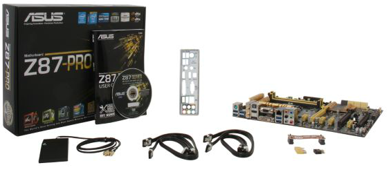
ASUS Z87-Pro In The Box
With an integrated WiFi module included in the package, no doubt the box will contain a WiFi antenna – in previous generations this would be a set of magnetized antennas to be positioned on a PC case at the users’ discretion. For Z87 the antenna shifts to a single device that can be positioned flat or perpendicular. Other than SATA cables and Q-Connectors our box is relatively bare:
Rear IO Panel
Driver Disk
User Guide
WiFi Antenna
Four SATA Cables
SLI Bridge
Q-Connectors
ASUS Z87-Pro Overclocking
Experience with ASUS Z87-Pro
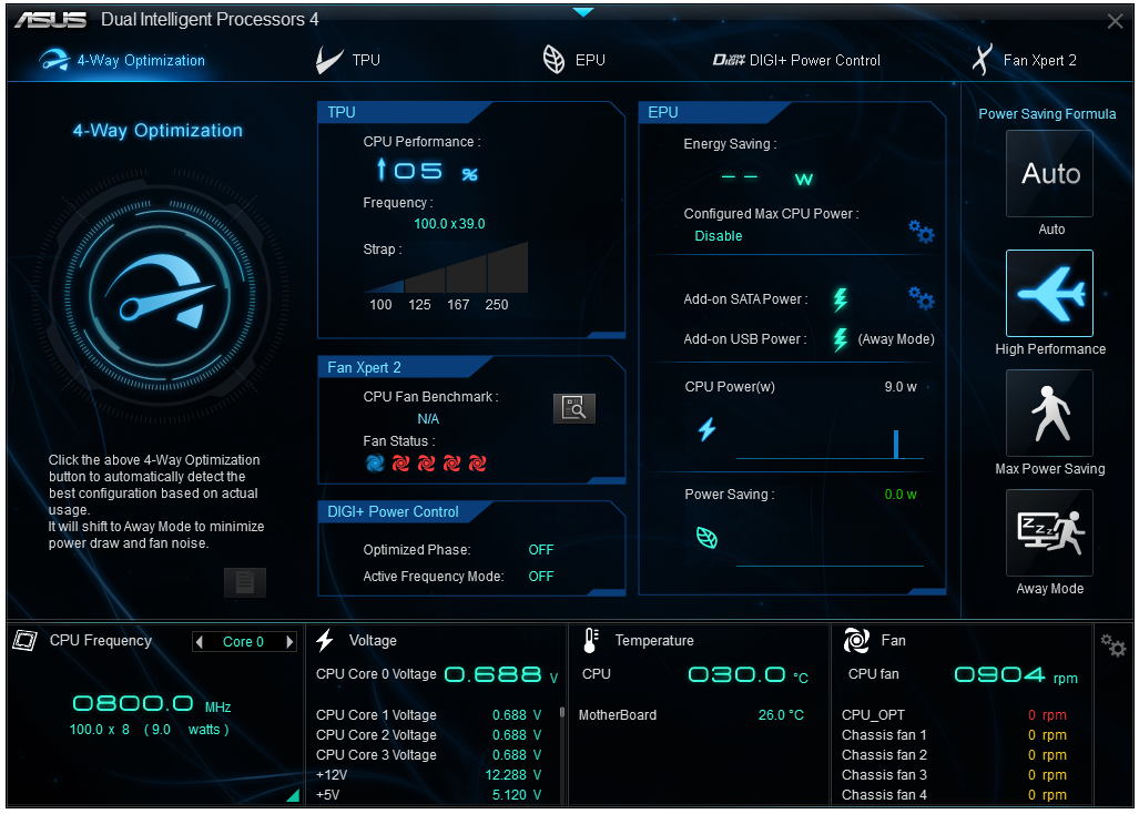
From previous reviews of ASUS motherboards, we typically have some of our best experiences on ASUS products – our recent review of the Maximus V Formula is one such example. Through the OS software we have the option of automatic tuning via DIP-IV, or manual adjustments of speeds, voltages and power control. TPU is also available via a two-stage DIP-switch on board, giving two different overclocks.
The BIOS is the place to head for manual overclocks, whereby the My Favorites menu allows the user to place the options they concern about the most into a single menu. For our overclock testing this usually means the VCore, the VRIN, Load Line Calibration, CPU Ratio and Memory Settings. Performance on the ASUS Z87-Pro matched the other motherboards in this test, whereby moving above 1.300 volts tends to increase peak temperatures by a significant amount.
Methodology:
Our standard overclocking methodology is as follows. We select the automatic overclock options and test for stability with PovRay and OCCT to simulate high-end workloads. These stability tests aim to catch any immediate causes for memory or CPU errors.
For manual overclocks, based on the information gathered from previous testing, starts off at a nominal voltage and CPU multiplier, and the multiplier is increased until the stability tests are failed. The CPU voltage is increased gradually until the stability tests are passed, and the process repeated until the motherboard reduces the multiplier automatically (due to safety protocol) or the CPU temperature reaches a stupidly high level (100ºC+). Our test bed is not in a case, which should push overclocks higher with fresher (cooler) air.
Automatic Overclock:
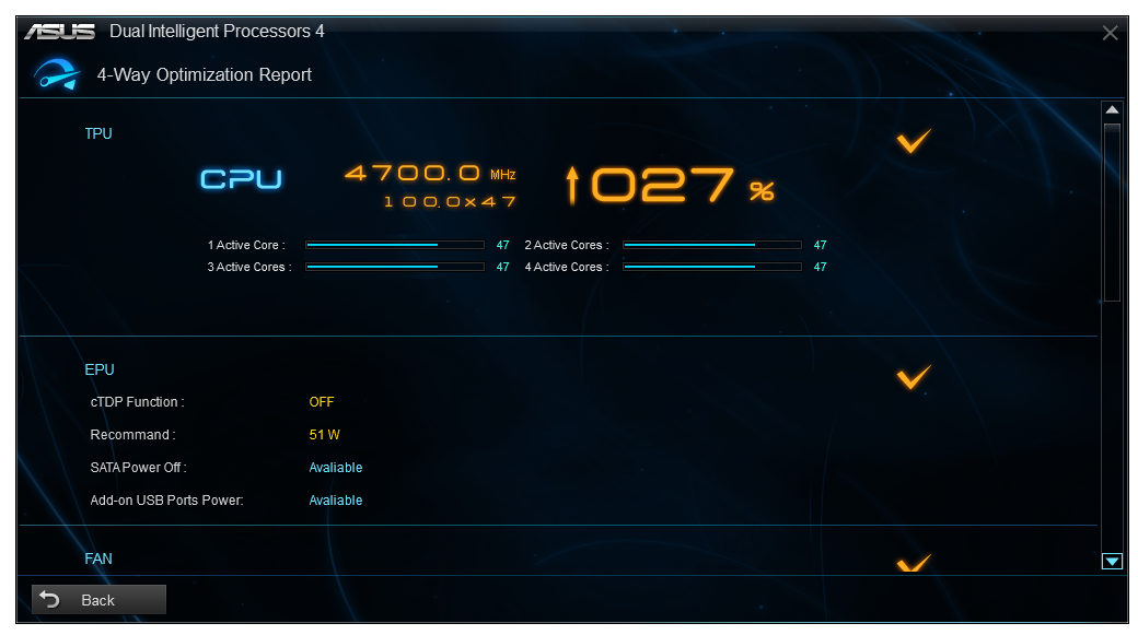
For our automatic overclock settings we tested the AI Suite III 4-Way Optimization option, which caters for speed, energy, digital power aggression and optimum fan speeds. The TPU Switch was also tested in both positions. Here are our results.
The 4-Way Optimization method performed a series of stress tests to increase the multiplier:
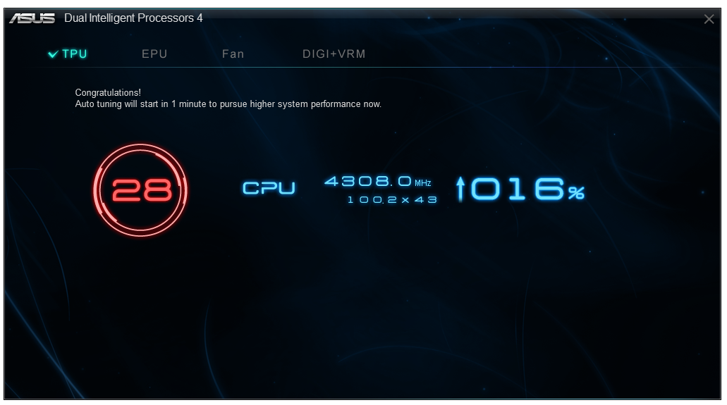
The system would restart, presumably to increase boot stability to push overclock in the operating system further. The final result was a nice and high 4.7 GHz:
At this setting the CPU was placed on a 1.250 volt setting with a 0.025 volt offset in Adaptive mode, with VRIN set to 1.81 volts and XMP enabled. With these settings, the system showed a load of 1.296 volts, a PovRay score of 1935.7 but caused a BSOD during OCCT. It has been noted that in Adaptive mode, artificial load generators can cause Haswell CPUs to request more voltage than would be requested during normal high-CPU activities such as video editing; this could be the reason for the OCCT test to fail.
With the TPU switch set to Level 1, the CPU was given a staggered multiplier setting of 43/43/42/41x at 1/2/3/4 core loading. The BIOS was automatically set to 1.150 volts with a 0.025 volt offset and a VRIN of 1.81 volts. At these settings, the system showed a load of 1.152 volts, a PovRay score of 1687.69 and an OCCT peak temperature of 72C. XMP was also applied.
With the TPU switch set to Level 2, the CPU was given a 34x125 overclock (4250 MHz) under all loading, with a CPU setting of 1.175 volts and a VRIN of 1.81 volts. With these settings, the system adjusted the memory from XMP (2400 10-12-12) to 2000 10-12-12 to compensate for the 125 MHz CPU strap, and then play it safe by reducing the memory strap. At these settings a CPU loading of 1.200 volts was observed, a PovRay score of 1749.74 and an OCCT peak temperature of 83C.
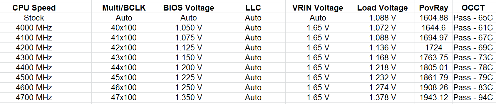
Manual Overclock:
Using the knowledge gained from previous testing, we set the VRIN to 1.65 volts and under ASUS’ recommendations left LLC on Auto. If ASUS have not already, there is an overclocking guide written by the technical guys within ASUS to aid in overclocking and how to deal with the old and new options in the new BIOS. Here are our results:


58 Comments
View All Comments
clyman - Tuesday, November 26, 2013 - link
In my personal experience and from ASUS tech support, the safest way to update bios is by first downloading it. This mobo has an excellent update program in bios that only looks at local drives, not online. I found it quite simple at each bios update.silenceisgolden - Thursday, June 27, 2013 - link
Great job Ian, really looking forward to the super high end motherboard review as well! I'm curious though, did you use the VGA port at all in any of these reviews, and also when was the last time you used a VGA port?IanCutress - Thursday, June 27, 2013 - link
My Korean 1440p panels are all via DVI-D. But the VGA comes in use when you have to use a DVI-I to VGA converter for DVI-I cables. Otherwise you need a DVI-D cable.JeBarr - Thursday, June 27, 2013 - link
Great review Ian. I very much appreciate your taking the time to explain the PCIe slot assignment and repeating the less-than-x8-no-good-for-SLI truth that needs to spread far and wide.What I took away from this review when analysing my own usage patterns and component choices is that each of the boards in this review would be better suited to the mATX form factor. There is no point in purchasing these mid-high end boards for multi-GPU, multi-display configs. There are only a handful of full size z87 boards that in my opinion earn their full-size status.
Shadowmaster625 - Thursday, June 27, 2013 - link
If it has fully integrated voltage regulators then why in blazes does it still need $20 worth of components buried beneath $3 heatsinks surrounding the cpu socket? Yeah, that's what I thought....DanNeely - Thursday, June 27, 2013 - link
What FIVR means to Intel isn't quite what you think it means. What's on package is the collection of VRs needed to provide power to all the separate sections of the CPU and to vary them as the chip clocks itself up and down. The motherboard itself still needs to do the heavy lifting to convert the 12V from the PSU to the voltage used by the DRAM and to a single input voltage the that CPU converts to the other levels it uses internally (IIRC this is the full load core voltage).I believe the reason why those regulators can be squeezed into the package while the ones still on the mobo are much larger is that the uncore/cache have relatively low power levels and the lower core voltages are only used at low CPU loads and thus don't need to push nearly as high of a peak current level.
WeaselITB - Thursday, June 27, 2013 - link
Wonderful review, Ian. Any chance of a Z87 vs Z77 vs ... comparison chart? It seems like functionalities of the processor are highly publicized, and the individual motherboard reviews chart the differences between chipset models within that family, but I don't recall seeing a comparison between chipset families. I know the chipset seems to be taking a smaller and smaller role these days, but it would still be helpful to exactly see the differences between generations.Thanks!
Kougar - Thursday, June 27, 2013 - link
It doesn't work with my 30" U3011 monitor either, yet another forum user with the same monitor didn't have any problem. Only difference was he used a Radeon and I use a GTX 480.
Creig - Thursday, June 27, 2013 - link
I only had time so far to skim this article, so I apologize if this question was already answered in the body. Is there any way to find out when each board starts shipping with the C2 stepping of the Z87 chipset? As some people are already aware, the C1 stepping has been shown to have issues with certain USB 3.0 controllers disconnecting when the computer awakes from sleep mode. The C2 stepping is apparently already shipping to manufacturers, but it would be handy to know a way to ensure that a person who orders a board in the near future receives the updated chipset.blackie333 - Friday, June 28, 2013 - link
I'm not sure that C2 stepping shipping already started, according to public available plan from May only samples have been sent to manufacturers. Mass production of C2 should start on 1st of July and manufacturers should start receiving them from the 30th of July. Boards based on C2 stepping should be available for end users from middle August.But you maybe have some more actual/insider information.