NVIDIA Tegra 4 Architecture Deep Dive, Plus Tegra 4i, Icera i500 & Phoenix Hands On
by Anand Lal Shimpi & Brian Klug on February 24, 2013 3:00 PM ESTNVIDIA has upped its ISP game with Tegra 4, and includes the same ISP in both Tegra 4 and 4i, which they’ve dubbed Chimera. This new ISP includes a number of features which were already demonstrated at CES, but NVIDIA went into greater detail.

NVIDIA’s major new feature with Tegra 4 is inclusion of new APIs which leverage the GPU to enable computational camera features In addition to the traditional ISP pipeline. To begin, NVIDIA has made their own enhancements in the imaging chain which leverage this GPU-assisted architecture that sits atop the normal ISP. They’ve outlined a few features which work atop this — HDR panorama, HDR stills, and real time object tracking. The end result is that Chimera is one part programming model and APIs for future development efforts by third parties, another part first party software that NVIDIA will distribute for integration in OEM cameras which includes the HDR features and object tracking.
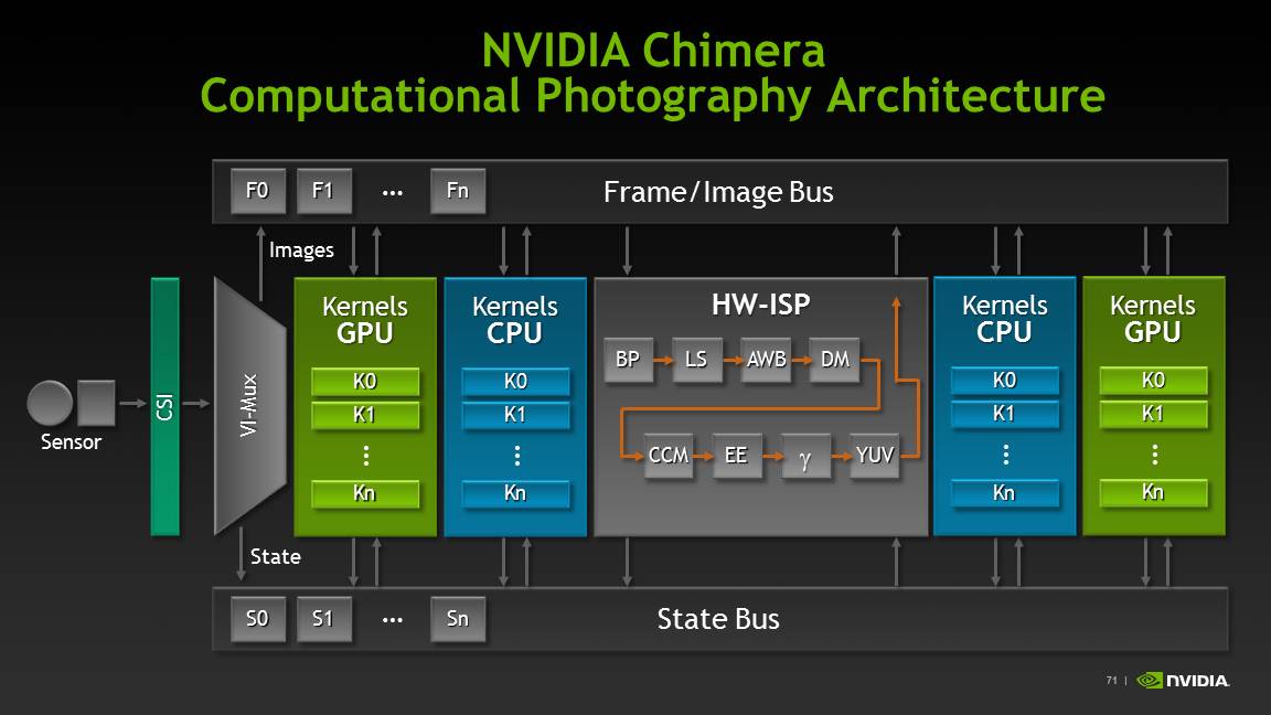
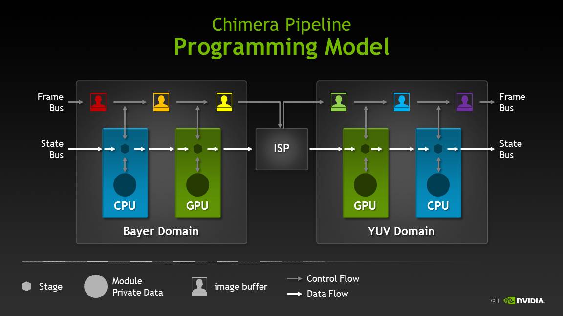
Chimera allows developers to build blocks around the traditional ISP data flow and get to manipulate either bayer image data or YUV space image data on the CPU or GPU using their own framework. There are still a lot of details to come about the programming model and how this will be exploited, but there clearly is space here for NVIDIA to try and make a case for their GPU being useful for image processing. At the same time, the elephant in the room is OpenCL (and its current absence on Tegra 4) and what direction the industry will take that to leverage GPU compute for some computational photography processing.
The novel new feature of note is something I was skeptical about upon seeing at CES — single frame HDR video. The traditional route for HDR video capture is to capture at twice the framerate of the intended output video, for example for 720p30 video with a two-frame HDR, that would mean capture at 720p60 with two different exposures. What NVIDIA does is a bit different. Instead of capturing two exposures and combining them after capture, NVIDIA has found a way to drive selected CMOS sensors (both IMX135 from Sony and AR0833 from Aptina have been called out specifically, but there are more) in some special fashion, and recombine interleaved high and low exposure images (the +1 stop, –1 stop) image into one equivalent frame. This is all done on the GPU using the same Chimera pipeline blocks, but with NVIDIA’s own algorithm. The results are actually pretty impressive, NVIDIA claims 3 stops of dynamic range (~24 dB), and no recombination artifacts.
Previous demonstrations of HDR video capture on a few other platform have had halos around moving elements because of the issues associated with taking two temporally different frames and recombining them. With NVIDIA’s HDR video capture I saw no halos even on very fast moving objects, with the same quality of HDR.
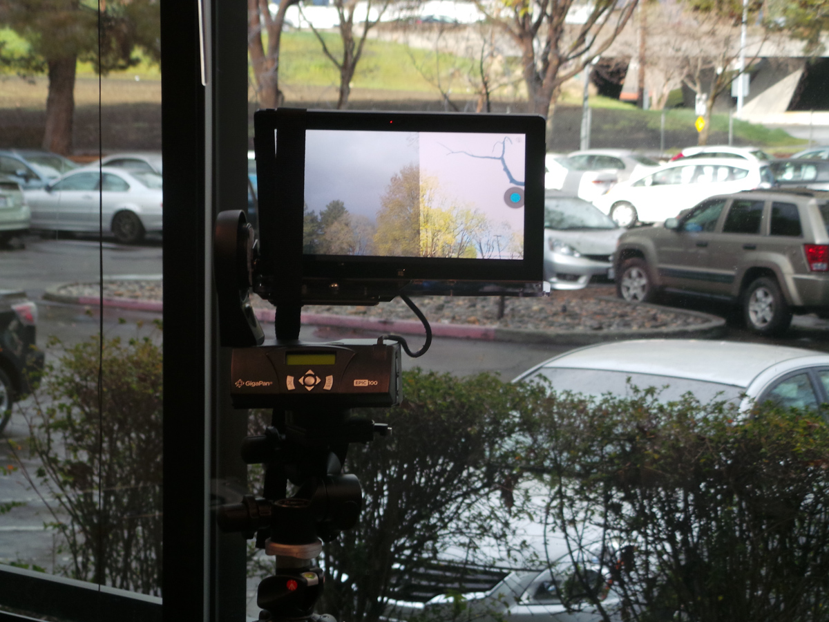
NVIDIA also demonstrated their panorama capture which includes HDR as well, using a GigaPan Epic 100. Admittedly a better demo might be hand held to demonstrate how well the ISP is able to compensate for change in perspective from the tablet moving around in the hand, the resulting image was the same quality of HDR as the still however. I also saw object tracking which essentially is face tracking (and thus AE / AF assist to that subject) but taken to arbitrary subjects. Paint a box around the object you want to track, and the camera will perform feature extraction and machine learn a model around the object. Rotating around complex geometries seemed to work decently well — the model learns slowly so slow movements can be accommodated, faster moving subjects might not be object tracked.

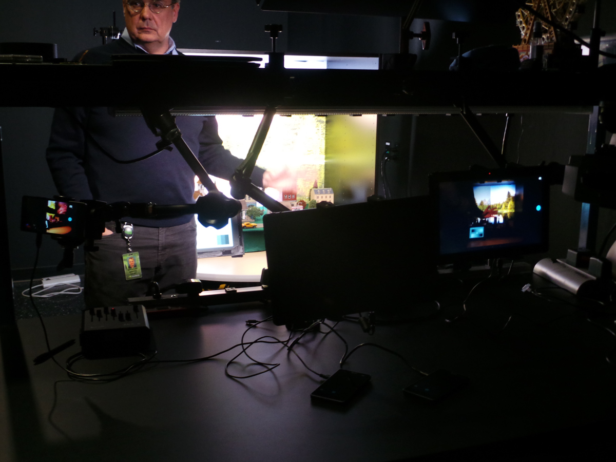
I also got a chance to tour NVIDIA’s camera tuning labs, where they characterize smartphone CMOSes for handset markers, and work with them on tuning their ISP and imaging experience. I saw one calibration room with many different scenes, and then another room with large test charts, and two sets of standard test scenes in lightboxes. The ever-familiar GMB color checker card and ISO12233 charts were everywhere as well.


75 Comments
View All Comments
PingviN - Monday, February 25, 2013 - link
Tegra made an operating loss of $150 million for fiscal year 2012, despite getting into both the Nexus 7 (the refresh coming this year has been lost to Qualcomm) and the Surface RT. Sales prognosis cut almost in half for the fiscal year 2013. To date, Nvidia hasn't had any profit coming out of Tegra and now it's in limbo mode until Tegra 4 is released because Tegra 3 gets smashed by it's competition.It's been a pretty crappy year for Tegra.
guilmon14 - Tuesday, February 26, 2013 - link
I don't know anything about this company "tegra", but have you heard about Nvidia? I heard they're doing great!http://nvidianews.nvidia.com/Releases/NVIDIA-Repor...
According to this Nvidia is up in income, revenue, and equity.
If you wanted to check the easy way just look at nvidia's wikipedia page, gives you all the nice money numbers.
http://en.wikipedia.org/wiki/Nvidia
trajan2448 - Monday, February 25, 2013 - link
5 years down the road phones will be cooking our dinner. It's amazing how fast the tech is advancing now.Scannall - Monday, February 25, 2013 - link
If they don't hustle right along, SOC's with the PowerVR 6 series (Rogue) will beat them to market. And considering their GPU just barely squeaks by the iPad as it is, it will be behind early on.Khato - Monday, February 25, 2013 - link
Was it specifically stated that the Tegra 4 SPECint/W figure was running on the high speed cores? As is mentioned later on the page, a SPECint2000 of 520 is within reach of the power optimized companion core, so the only reason I'd expect NVIDIA to not use the companion core for this data is if they explicitly stated that it wasn't.Part of the cause for my suspicion is that the Power vs DMIPS chart that Samsung recently provided for the Exynos 5 Octa shows 8k DMIPS at 1 watt... and from the press coverage back in 2009 for the A9 hard macros there's both the 10k DMIPS at 1.9 watts and 2GHz with the speed speed optimized and 4k DMIPS at 250 mW and 800 MHz for the power optimized. Which equate to 5.26 DMIPS/mW and 8 DMIPS/mW, respectively. Now the 2GHz data point should be even worse off than Tegra 3 and yet it only shows the Samsung Exynos 5 Octa as being 52% more efficient.
Going into estimating rather than published numbers, if we up the efficiency of Tegra 3 a bit compared to that 2GHz figure then it's likely going to be closer to A15 being 30% more efficient... which you then add the known ~40% efficiency bump going from a performance to power implementation and you get the kind of drastic increase NVIDIA is touting.
Wilco1 - Monday, February 25, 2013 - link
It doesn't matter whether they used the 5th core or one of the fast ones. By definition the cross over point is where the 5th core uses as much power as a fast core. Since that is ~800MHz, the power efficiency is the same. The 5th core can likely clock to well over 1GHz, but then it uses more power than a fast core.You are basically right that some of the 73% MIPS/W improvement comes from the 40-28nm process change. However the combined improvement of process and micro architecture means that you can use the low power core far more often. The 5th core in Tegra 4 is effectively more than 3 times as fast than the one in Tegra 3. So that means lots of tasks which needed 1-2 fast Tegra 3 cores can now run on the 5th Tegra 4 core. That means the power efficiency will actually improve by what NVidia suggests.
Khato - Monday, February 25, 2013 - link
Mind sharing the source for that? The wording in this article implies differently - "That 825MHz mark ends up being an important number, because that’s where the fifth companion Cortex A15 tops out at." Given 1.9GHz for the performance-optimized cores, something around 800 MHz sounds about right for the max frequency of a power-optimized version.Anyway, there's no question that Tegra 4 will be quite a bit more power efficient simply by virtue of being able able to run more workloads exclusively on the companion core. As said before, in exchange for a much lower cap on maximum frequency a power optimized synthesis gives at least a 40% bump in efficiency... and now that power optimized core will still deliver respectable performance.
Wilco1 - Monday, February 25, 2013 - link
Read http://www.nvidia.com/content/PDF/tegra_white_pape... it explains the difference between leakage and active power on low power and high performance transistors. It explicitly says the 5th core in Tegra is capped at 500MHz as that is where it is as power efficient as a fast core. The graphs and the word capped suggest the 5th core can go faster but there is no point.Note that Tegra 3 uses a different process with low power transistors for the 5th core rather than a low power synthesis (not that they couldn't have done that too, but it is never mentioned and the 5th core looks pretty much the same in the die plots). I presume Tegra 4 does the same on the 28nm process.
Khato - Tuesday, February 26, 2013 - link
Okay, so your commentary is based on the Tegra 3 which is using an entirely different approach to power savings for the companion core. Note that all of the data I was referencing for the difference in efficiency between ARM's two A9 hard macros was on the same process and hence is more applicable to the case of Tegra 4. As you correctly state, Tegra 3 gains its power efficiency for the companion core by using the LP process rather than a low power synthesis, likely due to it being a simpler and faster route to the desired end result and equally effective for their design goals.Tegra 4 isn't playing process games for the companion core. How do you gain efficiency on the same process? You loosen timings to allow for the usage of smaller transistors, less flop stages, so on so forth. The end result being that you sacrifice maximum switching speed to reduce both leakage and dynamic power. From all the information that NVIDIA has made available it's a completely different implementation from Tegra 3.
Wilco1 - Tuesday, February 26, 2013 - link
Tegra 4 does exactly the same as Tegra 3. According to NVidia's white paper on Tegra 4 (http://www.nvidia.com/docs/IO/116757/NVIDIA_Quad_a... it also uses low power transistors for the 5th core. Again if you look at the die photos of Tegra 4 all 5 cores are identical just like Tegra 3. So that seems to exclude a different synthesis.The way NVidia get a low power core is by using low power transistors. TSMC 28nm process supports several different transistor libraries, from high performance high leakage to low performance low leakage. Based on the information we have all they have done is swap the transistor libraries.