NVIDIA Tegra 4 Architecture Deep Dive, Plus Tegra 4i, Icera i500 & Phoenix Hands On
by Anand Lal Shimpi & Brian Klug on February 24, 2013 3:00 PM ESTSilicon makers almost always put together a reference design of their own for both testing their hardware, optimizing software stack, and generally having something to build to. Increasingly we’ve seen these vendors then take that reference design and do something with it beyond just having it for their own internal use — after all, if you’ve built and qualified a device, it makes sense to do something with it. While NVIDIA isn’t going to sell the FFRD directly, it’s a platform they can quickly hand off to OEMs wanting to implement a smartphone-platform with Tegra 4 or 4i relatively quickly.
To that end, NVIDIA has crafted Phoenix, which is their very own FFRD (Form Factor Reference Design) for both Tegra 4 and 4i versions. The high level specifications are what you’d expect for something from this current generation, with a 5-inch 1080p display, LTE, relatively thin profile, and of course a Tegra 4 SoC inside.
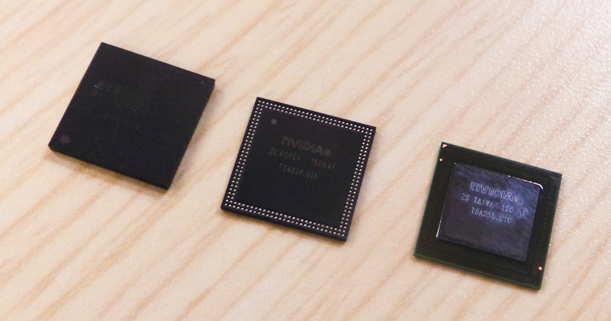
There are actually three different versions of the Phoenix — one in a version with Tegra 4, Tegra 4i without PoP (an external DRAM package), and a Tegra 4i version with PoP memory. All of them have the same PCB geometry inside, just a different SoC, and in the case of the Tegra 4 version, an external Icera i500 modem. NVIDIA showed us an image of their Tegra 4 Phoenix PCB, and in addition the Tegra 4i non PoP and Tegra 4 PCBs in the flesh. The Tegra 4 version has to include both Icera i500 and a MCP DRAM plus NAND of its own adjacent to it, right next to the DRAM for the Tegra 4. On the Tegra 4i version there’s simply unused space in the region occupied by those packages.
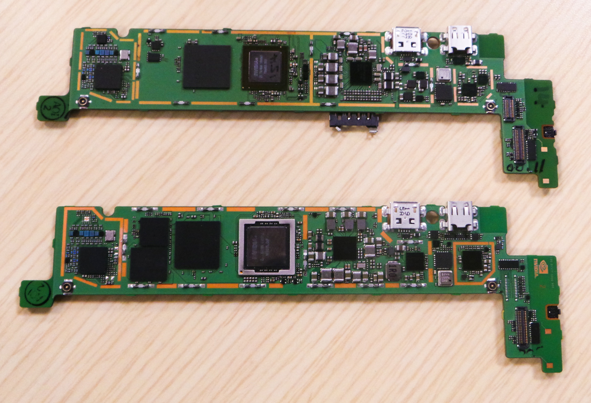
Glancing at the Tegra 4i package, we can also get Grey’s actual internal codename, which isn’t T30 series or T40 but rather T8A. The rest of the platform is basically what you’d expect for a modern device, and the PCB follows the rather typical L shaped design that’s common right now across the entire segment.


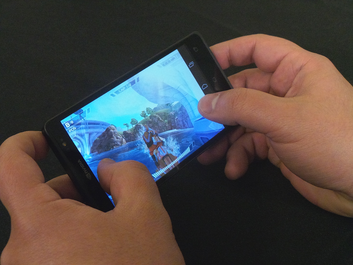
NVIDIA also showed a Tegra 4i based version of the Phoenix playing a version of Riptide 2 at 1080p with even more graphical assets (real time lighting, shadows, and improved water simulation) enabled over the previous version of Riptide optimized for Tegra 3.
I didn’t get too much time to play with the Phoenix – like any reference design from any of the players in this space it’s more of a function over form piece of equipment for developers or the silicon vendor themselves to get easy access to the insides – but superficially it’s the right kind of stuff for a smartphone right now.


75 Comments
View All Comments
Krysto - Monday, February 25, 2013 - link
S600 is just a slightly overclocked S4 Pro with the same GPU.The real competitor of Tegra 4 will be S800. We'll see if it wins in CPU performance (it might not), and I think there's a high chance it will lose in GPU performance, as Adreno 330 is only 50% faster than Adreno 320 I think, and Tegra 4 is about twice as fast.
Qualcomm has always had slower graphics performance than Nvidia actually. The only "gap" they found in the market was last fall with the Adreno 320, when Nvidia didn't have anything good to show. But Tegra 3 beat S4 with its Adreno 225.
watersb - Monday, February 25, 2013 - link
I'm amazed at the depth of this NVIDIA data-dump. Brilliant work.Anand's observation re: die size, cost strategy, position in the market and how this buys them time to consolidate... Wow.
Clearly, Nvidia is in this game for the long haul.
djgandy - Monday, February 25, 2013 - link
So OpenGL ES 3.0 doesn't matter, but quad core A15 does? Why do people suck up to Nvidia and their marketing BS so much?T4i still single channel memory? What a joke configuration.
djgandy - Monday, February 25, 2013 - link
Also a 9 page article about a mobile SoC without a single reference to the word "battery".varad - Monday, February 25, 2013 - link
Read the article before you write such comments. The very first page is "Introduction & Power" where they do mention some numbers and their thoughts.djgandy - Tuesday, February 26, 2013 - link
Yeah its all smoke and mirrors under lab test conditions. Where is the real battery life? Is this not for battery powered devices?Krysto - Monday, February 25, 2013 - link
Personally, I think all 2013 GPU's should have support for OpenGL ES 3.0 and OpenCL. I was stunned to find out Tegra 4 was not going to support it as they haven't even switched to a unified shader architecture.That being said, Anand is probably right that it was the right move for Nvidia, and they are just going to wait for the Maxwell architecture to streamline the same custom ARMv8 CPU from Tegra 5 to Project Denver across product line-ups, and also the same Maxwell GPU cores.
If that's indeed their plan, then switching Tegra 4 to Kepler this year, only to switch again to Maxwell next year wouldn't have made any sense. GPU architectures barely change even every 2-3 years, let alone 1 year. It wouldn't have been cost effective for them.
I do hope they aren't going to delay the transition again with Tegra 5 though, and I also do hope they follow Qualcomm's strategy with S4 last year of switching IMEMDIATELY to the 20nm process, instead of continuing on 28nm with Tegra 5, like they did with Tegra 3 on 40nm. But I fear Nvidia will repeat the same mistake.
If they put Tegra 5 on 20nm, and make it 120mm2 in size, with Maxwell GPU core, I don't think even Apple's A8X will stand against it next year in terms of GPU performance (and of course it will get beaten easily in CPU performance, just like this year).
djgandy - Tuesday, February 26, 2013 - link
Tegra is smaller because it lacks features and also memory bandwidth. The comparison is not really fair to assume you can just throw more shaders at the problem. You'll need wider memory bus for a start. You'll need more TMU's and in the future it's probably smart to have a dedicate ROP unit. Then also are you seriously going to just stick with FP20 and not support ES 3.0 and OpenCL? OEMs see OpenCL as a de facto feature these days, not because it is widely used but because it opens up future possibilities. Nvidia has simply designed an SoC for gaming here.Your post focuses on performance, but these are battery powered devices. The primary design goal is efficiency, and it would appear that is why apple went swift and not A15. A15 is just too damn power hungry, even for a tablet.
metafor - Tuesday, February 26, 2013 - link
If the silicon division of Apple were its own business, they'd be in the red. Very few silicon providers can afford to make 120mm^2 chips and still make a profit; let alone one with as little bargaining clout in the mobile space as nVidia.Numbers are great but at the end of the day, making money is what matters.
milli - Monday, February 25, 2013 - link
nVidia is trying hard but Tegra still isn't making them any money ...