NVIDIA Tegra 4 Architecture Deep Dive, Plus Tegra 4i, Icera i500 & Phoenix Hands On
by Anand Lal Shimpi & Brian Klug on February 24, 2013 3:00 PM ESTCortex A15 Architecture
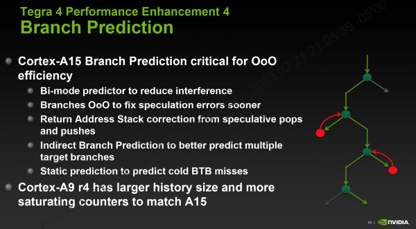
I want to go deeper into ARM’s Cortex A15 but I’ll have to save that for another time. At a high level you’re looking at a much deeper, much wider architecture than the Cortex A9. The integer pipeline is significantly deeper (15 stages vs. 9 stages), however branch prediction has been improved considerably to hopefully offset the difference.
The front end is 50% wider and has double the instruction fetch bandwidth of the Cortex A9, which helps increase instruction level parallelism. In order to capitalize on the 3-wide machine, ARM dramatically increased the size of the reorder buffer and all associated data structures within the machine. While the Cortex A9 could keep around 32 - 40 decoded instructions in its reorder buffer, Cortex A15 can hold 128 - an increase of up to 4x. The larger ROB alone gives you a good idea of the magnitude of difference between the Cortex A9 and A15. While the former was a natural evolution over the Cortex A8, ARM’s Cortex A15 is really a leap forward both in performance and power consumption - clearly aimed at something much more than just smartphones.
Getting to the execution core, A15 continues the trend of being considerably wider than A9. There are more execution ports and more execution units, all of which help to increase ILP/single threaded performance. ARM went to multiple, independent issue queues in order to keep frequencies high. Each issue queue can accept up to three instructions and all issue queues can dispatch in parallel.
The A15 can execute instructions out of order like the A9, however its abilities grow quite a bit. All FP/NEON instructions had to be executed in-order on Cortex A9, but they can now be executed OoO in the A15. Despite the beefier OoO execution engine, the Cortex A15 can’t reorder all memory operations (independent loads can be executed out of order, but stores can’t be completed ahead of loads).
The Cortex A15 moves back to an integrated L2 cache structure, rather than a separate IP block as was the case with the Cortex A9. L1 and L2 cache latencies remain largely unchanged, although I do believe A15 does see a 1 - 2 cycle penalty over A9 in a few cases. The level 2 TLB and other data structures grow in size considerably in order to feed the hungrier machine.
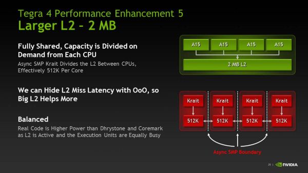
Although the L1 caches remain the same size as NVIDIA’s Cortex A9 (32KB I + 32KB D), the the L2 cache grows to 2MB. The 2MB L2 is shared by all four cores (the companion core has its own private 512KB L2), and any individual core can occupy up to the entire 2MB space on its own. Alternatively, all four cores can evenly share and access the large L2.


75 Comments
View All Comments
Death666Angel - Wednesday, February 27, 2013 - link
Get a life.StormyParis - Sunday, February 24, 2013 - link
I'd go with Anand, anytime. Charlie is a raving bitch.mayankleoboy1 - Sunday, February 24, 2013 - link
Except that this raving bitch has accurately predicted the future course of most companies months before anybody.Avalon - Monday, February 25, 2013 - link
If by accurate you mean he made many predictions for every company and when one of the predictions came true everyone forgot about all the wrong ones. He guesses.Kiste - Monday, February 25, 2013 - link
Confirmation bias ahoy!AmdInside - Monday, February 25, 2013 - link
Are you kidding me? Even congress lies less than Charlie does.jjj - Sunday, February 24, 2013 - link
I wouldn't expect a huge downclock for phones , they do need to limit heat, not going with POP for the RAM helps ,some actual cooling (air gap or metal) could also be used so they will most likely allow 1-2 cores to go pretty high and maybe all 4 for short periods of time (so the usual tricks to get more out of it).R3MF - Sunday, February 24, 2013 - link
re tegra 4 gpu architecture.how did you get through this many words without mentioning OpenCL?
lack of ES 3.0 is only half the problem.
cmikeh2 - Sunday, February 24, 2013 - link
He does reference it when discussing the Chimera ISP:"At the same time, the elephant in the room is OpenCL (and its current absence on Tegra 4) and what direction the industry will take that to leverage GPU compute for some computational photography processing."
guidryp - Sunday, February 24, 2013 - link
The Icera acquisition was a brilliant one. This gives NVidia the complete mobile package. It will be very interesting to see how this works out in practice. NVidia is a fierce competitor, Qualcomm should be worried.