The Tegra 4 GPU, NVIDIA Claims Better Performance Than iPad 4
by Anand Lal Shimpi on January 14, 2013 6:13 PM ESTAt CES last week, NVIDIA announced its Tegra 4 SoC featuring four ARM Cortex A15s running at up to 1.9GHz and a fifth Cortex A15 running at between 700 - 800MHz for lighter workloads. Although much of CEO Jen-Hsun Huang's presentation focused on the improvements in CPU and camera performance, GPU performance should see a significant boost over Tegra 3.
The big disappointment for many was that NVIDIA maintained the non-unified architecture of Tegra 3, and won't fully support OpenGL ES 3.0 with the T4's GPU. NVIDIA claims the architecture is better suited for the type of content that will be available on devices during the Tegra 4's reign.
Despite the similarities to Tegra 3, components of the Tegra 4 GPU have been improved. While we're still a bit away from a good GPU deep-dive on the architecture, we do have more details than were originally announced at the press event.
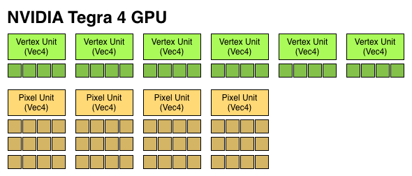
Tegra 4 features 72 GPU "cores", which are really individual components of Vec4 ALUs that can work on both scalar and vector operations. Tegra 2 featured a single Vec4 vertex shader unit (4 cores), and a single Vec4 pixel shader unit (4 cores). Tegra 3 doubled up on the pixel shader units (4 + 8 cores). Tegra 4 features six Vec4 vertex units (FP32, 24 cores) and four 3-deep Vec4 pixel units (FP20, 48 cores). The result is 6x the number of ALUs as Tegra 3, all running at a max clock speed that's higher than the 520MHz NVIDIA ran the T3 GPU at. NVIDIA did hint that the pixel shader design was somehow more efficient than what was used in Tegra 3.
If we assume a 520MHz max frequency (where Tegra 3 topped out), a fully featured Tegra 4 GPU can offer more theoretical compute than the PowerVR SGX 554MP4 in Apple's A6X. The advantage comes as a result of a higher clock speed rather than larger die area. This won't necessarily translate into better performance, particularly given Tegra 4's non-unified architecture. NVIDIA claims that at final clocks, it will be faster than the A6X both in 3D games and in GLBenchmark. The leaked GLBenchmark results are apparently from a much older silicon revision running no where near final GPU clocks.
| Mobile SoC GPU Comparison | |||||||||||||||
| GeForce ULP (2012) | PowerVR SGX 543MP2 | PowerVR SGX 543MP4 | PowerVR SGX 544MP3 | PowerVR SGX 554MP4 | GeForce ULP (2013) | ||||||||||
| Used In | Tegra 3 | A5 | A5X | Exynos 5 Octa | A6X | Tegra 4 | |||||||||
| SIMD Name | core | USSE2 | USSE2 | USSE2 | USSE2 | core | |||||||||
| # of SIMDs | 3 | 8 | 16 | 12 | 32 | 18 | |||||||||
| MADs per SIMD | 4 | 4 | 4 | 4 | 4 | 4 | |||||||||
| Total MADs | 12 | 32 | 64 | 48 | 128 | 72 | |||||||||
| GFLOPS @ Shipping Frequency | 12.4 GFLOPS | 16.0 GFLOPS | 32.0 GFLOPS | 51.1 GFLOPS | 71.6 GFLOPS | 74.8 GFLOPS | |||||||||
Tegra 4 does offer some additional enhancements over Tegra 3 in the GPU department. Real multisampling AA is finally supported as well as frame buffer compression (color and z). There's now support for 24-bit z and stencil (up from 16 bits per pixel). Max texture resolution is now 4K x 4K, up from 2K x 2K in Tegra 3. Percentage-closer filtering is supported for shadows. Finally, FP16 filter and blend is supported in hardware. ASTC isn't supported.
If you're missing details on Tegra 4's CPU, be sure to check out our initial coverage.


59 Comments
View All Comments
BugblatterIII - Monday, January 14, 2013 - link
Well there's also the IO sub-system, which tends to be very slow in many devices.I don't know what Apple devices are like, but IO performance is the biggest problem with my Transformer Prime. A fast CPU doesn't help if it's twiddling its thumbs waiting for data.
BugblatterIII - Monday, January 14, 2013 - link
Well obviously I want it all; their job is to make them faster at the same or lower power.To be fair if Tegra 4 goes into phones it should be far faster than the A6 (PowerVR SGX543MP3) in the iPhone 5, I'd just like something available for tablets that'd beat the iPad 4, especially since Android high-res tablets are likely to have more pixels to push (e.g. Nexus 10).
bpear96 - Saturday, January 26, 2013 - link
Now that android has all the hardware acceleration going on, a faster more powerful GPU will not only be good for games, but really smooth out the whole OSdragonsqrrl - Monday, January 14, 2013 - link
The GPU in the A6X represents the maximum configuration for the SGX554, the same is true for the 543 in the A5X. There's a reason you don't see MP4 554's or 543's in smartphone form factors. These are high die area, high power consumption GPU configurations. There are tradeoffs.I think the fact that Nvidia was able to match the theoretical FP performance of Power VR's highest end options at a lower transistor count and substantially lower die size is in itself impressive. If we see Tegra 4 in smartphones, which I'm assuming we will, it'll be quite an impressive accomplishment to say the least.
I'm not sure why this is never a part of the conversation when discussing the value of a mobile SOC, but all the performance the SGX 543 and 554 offer also comes at the price of comparatively high transistor counts and high power consumption. The A5X and A6x at load consume a LOT of power, due in large part to their GPU's. Tegra 3 was clearly never meant to compete with an A5X or A6X, which is why I've always been a bit confused when the anti-Tegra 3 bandwagon would draw comparisons.
Zink - Monday, January 14, 2013 - link
There is obviously an advantage to big die to offset the downside of increased cost or no one would design a big chip for mobile devices. I think the explanation is that high transistor count actually allows for low clockspeeds (lower votage) and efficiency. A5X and A6X run at about 250 MHz while Tegra 3 clocks over 500 Mhz. If it was really more efficient to run small chips like 554 MP2 at high clocks then why would we have MP4?dragonsqrrl - Monday, January 14, 2013 - link
They're completely different architectures, and the optimal clock ranges for a ULP geforce and SGX554 probably vary. I could turn your question around and ask why Apple wouldn't simply use lower clocked versions of an A5X or A6X in their iPhones? There's probably some threshold for a given form factor where it becomes more practical to either add more hardware units, or raise clocks on fewer units to achieve a certain performance target. Take the SGX543 MP3 in the A6 for example.There's probably some benefit for Apple to take the larger die size approach for their tablet form factor, I'm just not sure it's mainly for power efficiency. Perhaps its simply because they have that additional thermal headroom to work with in an SOC designed specifically for tablets?
Zink - Monday, January 14, 2013 - link
I agree that the optimal clock ranges are probably different. If you have to ask the main downsides of using a big die that I can think of would be cost, production time, and motherboard real estate. SGX544 (basically SGX543) is run at 384 MHz in shipping hardware so there is no question that it can go higher. The main benefit of a big die is power efficiency but I can’t find that mentioned in any of Anand’s Apple reviews.But Tegra does suck compared to Apple hardware from the same generation. :p
Zink - Monday, January 14, 2013 - link
1. From what I understand, SGXMP4 is not inherently high power consumption. I think that die area alone is the reason Apple (the only one using SOCs that big in tablets) does not put these chips in phones and that they would be just as power efficient as any other current GPU when run at 1.5W. There are tradeoffs yes, likely cost and motherboard real estate.2. I disagree that Nvidia using a smaller die at higher clocks to match current PowerVR performance is impressive with no power consumption numbers to back it up. Tegra 4 needs to be efficient at low power to do well in phones and we still don’t know how it will perform in that regard.
3. The only tablets with these hot chips are the iPads which provide a fat battery and better gaming battery life than competing devices. Tegra 3 is also an equally hot chip, if you crunch the gaming power consumption numbers in the AT TF700T review, T33 is drawing about 30% more power than A5X and going much slower.
4 . You are right that Tegra 3 is a cheaper small die part that does not compete with the big high cost MP4 chips.
TLDR; there is good reason the the anti-Tegra bandwagon when cost is not being considered
fm123 - Tuesday, January 15, 2013 - link
Apple doesn't have to care about die size so much, because they don't need to sell to others. Plus they have dedicated fabs for their parts. Nvidia is making one part that is being used for both tablet and phone applications, so they don't have the option like Apple of making two size parts. They went with an optimal compromise on size and what could fit in there. A6X is around 30%+ larger than T4, even accounting for fab size.milli - Tuesday, January 15, 2013 - link
Indeed and this is the part that people seem to ignore. Apple SOC's cost much more to produce but all Apple needs to worry about is the total BOM. While NVidia actually needs to sell these SOC's and try to make a profit on the chip itself (which it's failing to do ATM). Ex.: A6 costs $20 to produce but HTC needs to pay nVidia $25 for T3.Apple can make profit much easier since they're making the full device (and can charge up to $100 for 16GB of NAND!). R&D costs of developing such SOC's become a small fraction of the total cost when you produce close to 200 million units a year.
The only other company in the same position as Apple is Samsung (actually in a better position since they own the fabs (chip, screen, ...) too) and they're moving to bigger SOC's too.