Intel's Haswell Architecture Analyzed: Building a New PC and a New Intel
by Anand Lal Shimpi on October 5, 2012 2:45 AM ESTThe Haswell Front End
Conroe was a very wide machine. It brought us the first 4-wide front end of any x86 micro-architecture, meaning it could fetch and decode up to 4 instructions in parallel. We've seen improvements to the front end since Conroe, but the overall machine width hasn't changed - even with Haswell.
Haswell leaves the overall pipeline untouched. It's still the same 14 - 19 stage pipeline that we saw with Sandy Bridge depending on whether or not the instruction is found in the uop cache (which happens around 80% of the time). L1/L2 cache latencies are unchanged as well. Since Nehalem, Intel's Core micro-architectures have supported execution of two instruction threads per core to improve execution hardware utilization. Haswell also supports 2-way SMT/Hyper Threading.
The front end remains 4-wide, although Haswell features a better branch predictor and hardware prefetcher so we'll see better efficiency. Since the pipeline depth hasn't increased but overall branch prediction accuracy is up we'll see a positive impact on overall IPC (instructions executed per clock). Haswell is also more aggressive on the speculative memory access side.
The image below is a crude representation I put together of the Haswell front end compared to the two previous tocks. If you click the buttons below you'll toggle between Haswell, Sandy Bridge and Nehalem diagrams, with major changes highlighted.
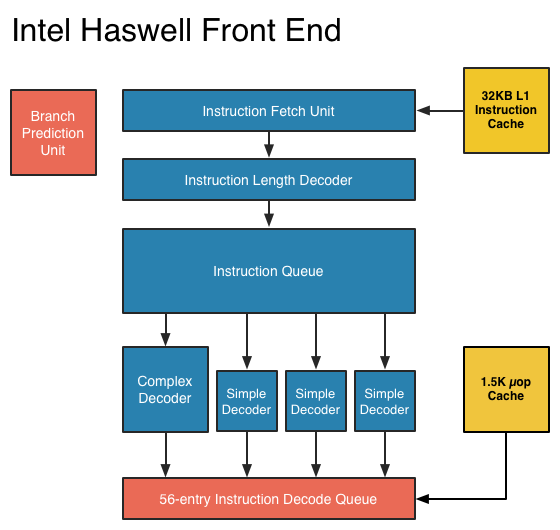
In short, there aren't many major, high-level changes to see here. Instructions are fetched at the top, sent through a bunch of steps before getting to the decoders where they're converted from macro-ops (x86 instructions) to an internally understood format known to Intel as micro-ops (or µops). The instruction fetcher can grab 4 - 5 x86 instructions at a time, and the decoders can output up to 4 micro-ops per clock.
Sandy Bridge introduced the 1.5K µop cache that caches decoded micro-ops. When future instruction fetch requests are made, if the instructions are contained within the µop cache everything north of the cache is powered down and the instructions are serviced from the µop cache. The decode stages are very power hungry so being able to skip them is a boon to power efficiency. There are also performance benefits as well. A hit in the µop cache reduces the effective integer pipeline to 14 stages, the same length as it was in Conroe in 2006. Haswell retains all of these benefits. Even the µop cache size remains unchanged at 1.5K micro-ops (approximately 6KB in size).
Although it's noted above as a new/changed block, the updated instruction decode queue (aka allocation queue) was actually one of the changes made to improve single threaded performance in Ivy Bridge.
The instruction decode queue (where instructions go after they've been decoded) is no longer statically partitioned between the two threads that each core can service.
The big changes in Haswell are at the back end of the pipeline, in the execution engine.


245 Comments
View All Comments
defiler99 - Tuesday, October 16, 2012 - link
One of the best articles on Anandtech in some time. This is great original tech industry reporting.Gc - Saturday, January 12, 2013 - link
Congratulations, an intel cpu engineer wrote around 27 Dec 2012:"... Anandtech's latest Haswell preview is also excellent; missing some key puzzle pieces to complete the picture and answer some open questions or correct some details but otherwise great. ..."
http://www.reddit.com/r/IAmA/comments/15iaet/iama_...
xaml - Thursday, May 23, 2013 - link
This was first posted here a few handfuls of pages back as a comment by user "telephone". ^^yhselp - Friday, March 29, 2013 - link
A few questions.Is there going to be a replacement (37W) for the current IVB 35W quad-core part? Quite a few designs are now dependable on this, lower power quad-core option - Sony S-series and Razer Blade, to name a few.
When can we expect all mobile CPUs (except maybe for the extreme series) to fall into the 10W-20W range? In three years' time and 10nm?
The decision to not include GT3 with desktop parts is very disappointing. A 35/45W low-voltage part with GT3 would make for an excellent HTPC build, among other things. Is there a chance Intel change their mind and start shipping GT3 desktop parts at some point?
JVimes - Tuesday, August 19, 2014 - link
Does EU stand for Execution Unit? That was surprisingly hard to google for.