Intel's Haswell Architecture Analyzed: Building a New PC and a New Intel
by Anand Lal Shimpi on October 5, 2012 2:45 AM ESTTSX
Johan did a great job explaining Haswell's Transactional Synchronization eXtensions (TSX), so I won't go into as much depth here. The basic premise is simple, although the implementation is quite complex.
It's easy to demand well threaded applications from software vendors, but actually implementing code that scales well across unlimited threads isn't easy. Parallelizing truly independent tasks is the low hanging fruit, but it's the tasks that all access the same data structure that can create problems. With multiple cores accessing the same data structure, running independent of one another, there's the risk of two different cores writing to the same part of the same structure. Only one set of data can be right, but dealing with this concurrent access problem can get hairy.

The simplest way to deal with it is simply to lock the entire data structure as soon as one core starts accessing it and only allow that one core write access until it's done. Other cores are given access to the data structure, but serially, not in parallel to avoid any data integrity issues.
This is by far the easiest way to deal with the problem of multiple threads accessing the same data structure, however it also prevents any performance scaling across multiple threads/cores. As focused as Intel is on increasing single threaded performance, a lot of die area goes wasted if applications don't scale well with more cores.
Software developers can instead choose to implement more fine grained locking of data structures, however doing so obviously increases the complexity of their code.
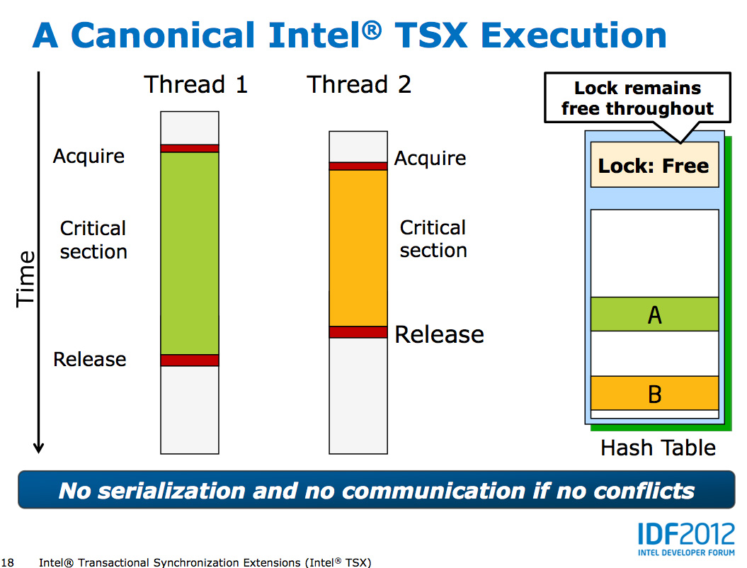
Haswell's TSX instructions allow the developer to shift much of the complexity of managing locks to the CPU. Using the new Hardware Lock Elision and its XAQUIRE/XRELEASE instructions, Haswell developers can mark a section of code for transactional execution. Haswell will then execute the code as if no hardware locks were in place and if it completes without issues the CPU will commit all writes to memory and enjoy the performance benefits. If two or more threads attempt to write to the same area in memory, the process is aborted and code re-executed traditionally with locks. The XAQUIRE/XRELEASE instructions decode to no-ops on earlier architectures so backwards compatibility isn't a problem.

Like most new instructions, it's going to take a while for Haswell's TSX to take off as we'll need to see significant adoption of Haswell platforms as well as developers embracing the new instructions. TSX does stand to show improvements in performance anywhere from client to server performance if implemented however, this is definitely one to watch for and be excited about.
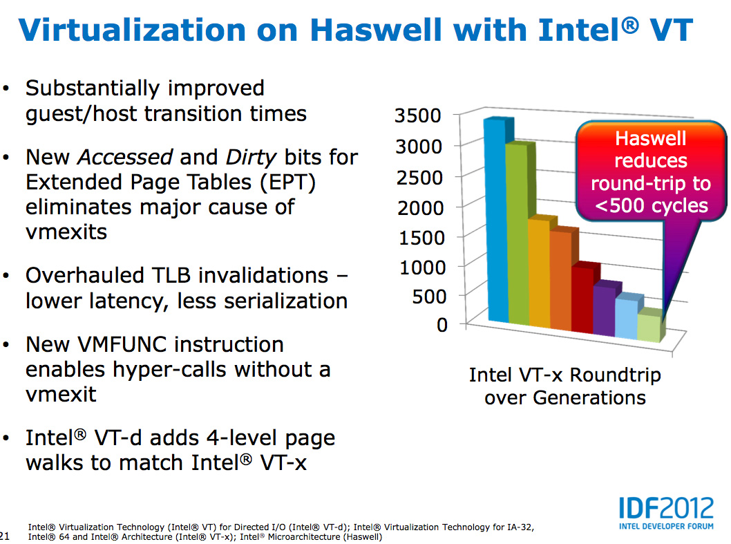
Haswell also continues improvements in virtualization performance, including big decreases to guest/host transition times.


245 Comments
View All Comments
random2 - Saturday, October 6, 2012 - link
"The race to the bottom that we've seen in the LCD space made it unlikely that any of the panel vendors would be jumping at the opportunity to make their products more expensive."It's unfortunate, because of what might have been had the manufacturers, of which there are only three main ones, if I recall, had the foresight to market to customers that weren't just looking to buy the lowest priced panel on display at Best Buy. Had they the initiative to have started years ago, there would be some pretty fantastic panels available today for much more reasonable prices than seen for the 27 and 30 inch 2560X1600 panels today.
Klugfan - Saturday, October 6, 2012 - link
This doesn't really belong in the Haswell article, but I would love to know more about the physics and constraints of TDP. Like, hit me with a chart of TDP impact for a variety of important parts in phones, tablets, laptops, and desktops. Show me a chart of TDP budgets and mitigation strategies. Explain to me roughly how physics forces those things to relate. Please.Seems important and it's easy to understand the comparison from Ivy Bridge to Haswell but that doesn't feel like the big picture.
havoti97 - Saturday, October 6, 2012 - link
I read the 1st page then got bored. Writing style is overly wordy... am I the only the feeling this way?xeizo - Saturday, October 6, 2012 - link
It's an article, not a twitter feed! Some of us like to get the whole picture not just the flashy stuff ....watersb - Saturday, October 6, 2012 - link
Phenomenal feature, Anand! This is why I check your site each day. Thanks very much!bill4 - Saturday, October 6, 2012 - link
like atom, you're stuck in no mans land. way too high for tablets and phones, but in desktops and laptop, who cares if the amd solution uses 30 watts instead of 8? that difference isn't enough to matter when you take the whole platform into account, especially at lower price points where battery life wont be fantastic anyway. on the dsktop it's completely pointless.JlHADJOE - Sunday, October 7, 2012 - link
On a laptop using 30 watts instead of 8 will more than triple your battery life, especially at lower price points/smaller form factors where manufacturers gimp the battery.How's about browsing for 9 hours instead of 3? Or 27 hours instead of 9? I'd jump on it in a heartbeat.
1008anan - Saturday, October 6, 2012 - link
Haswell will sport 32 single precision or 16 double precision flops per cycle per core for its desktop and high tdp mobile skews [at least 30 watt and up].Can anyone speculate on how many single precision and double precision flops per cycle per core Haswell will execute for its low TDP skews? For example the less than 10 watt skews? the 15 watt skews?
I would also be interested in learning speculation about how many execution units (or shader cores if you prefer standard nomenclature) the low TDP Haswell products will have.
1008anan - Saturday, October 6, 2012 - link
Haswell will be able to execute 16 double precision or 32 single precision flops per clock per core for desktop and high TDP mobile skews [at least 30 watts and up].Can anyone speculate on how many flops per cycle per core the sub 10 watt and 15 watt Haswell skews will execute? Similarly I would be interested in hearing speculation about how many graphic execution units (shader cores) the sub 10 watt and 15 watt Haswell products will come with. Any speculation on graphics clock speed?
Is it possible that the high end tock 22 nm Xeon server parts could have 32 double precision or 64 single precision flops per clock per core?
Laststop311 - Saturday, October 6, 2012 - link
Best explanation of haswell I've read to date. Good Job Anand.