Intel's Haswell Architecture Analyzed: Building a New PC and a New Intel
by Anand Lal Shimpi on October 5, 2012 2:45 AM ESTHaswell's Wide Execution Engine
Conroe introduced the six execution ports that we've seen used all the way up to Ivy Bridge. Sandy Bridge saw significant changes to the execution engine to enable 256-bit AVX operations but without increasing the back end width. Haswell does a lot here.
Just as before, I put together a few diagrams that highlight the major differences throughout the past three generations for the execution engine.
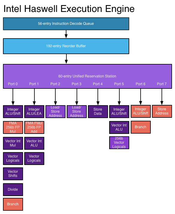
The reorder buffer is one giant tracking structure for all of the micro-ops that are in various stages of execution. The size of this buffer is directly impacted by the accuracy of the branch predictor as that will determine how many instructions can be kept in flight at a given time.
The reservation station holds micro-ops as they wait for the data they need to begin execution. Both of these structures grow by low double-digit percentages in Haswell.
Simply being able to pick from more instructions to execute in parallel is one thing, we haven't seen an increase in the number of parallel execution ports since Conroe. Haswell changes that.
From Conroe to Ivy Bridge, Intel's Core micro-architecture has supported the execution of up to six micro-ops in parallel. While there are more than six execution units in the system, there are only six ports to stacks of execution units. Three ports are used for memory operations (loads/stores) while three are on math duty. Over the years Intel has added additional types and widths of execution units (e.g. Sandy Bridge added 256-bit AVX operations) but it hasn't strayed from the 6 port architecture.
Haswell finally adds two more execution ports, one for integer math and branches (port 6) and one for store address calculation (port 7). Including both additional compute and memory hardware is a balanced decision on Intel's part.
The extra ALU and port does one of two things: either improve performance for integer heavy code, or allow integer work to continue while FP math occupies ports 0 and 1. Remember that Haswell, like its predecessors, is an SMT design meaning each core will see instructions from up to two threads at the same time. Although a single app is unlikely to mix heavy vector FP and integer code, it's quite possible that two applications running at the same time may produce such varied instructions. Having more integer ALUs is never a bad thing.
Also using port 6 is another unit that can handle x86 branch instructions. Branch heavy code can now enjoy two independent branch units, or if port 0 is occupied with other math the machine can still execute branches on port 6. Haswell moved the original Core branch unit from port 5 over to port 0, the most capable port in the system, so a branch unit on a lightly populated port makes helps ensure there's no performance regression as a result of the change.
Sandy Bridge made ports 2 & 3 equal class citizens, with both capable of being used for load or store address calculation. In the past you could only do loads on port 2 and store addresses on port 3. Sandy Bridge's flexibility did a lot for load heavy code, which is quite common. Haswell's dedicated store address port should help in mixed workloads with lots of loads and stores.
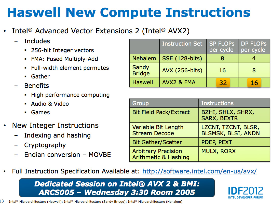
The other major addition to the execution engine is support for Intel's AVX2 instructions, including FMA (Fused Multiply-Add). Ports 0 & 1 now include newly designed 256-bit FMA units. As each FMA operation is effectively two floating point operations, these two units double the peak floating point throughput of Haswell compared to Sandy/Ivy Bridge. A side effect of the FMA units is that you now get two ports worth of FP multiply units, which can be a big boon to legacy FP code.
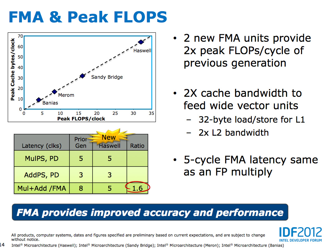
Fused Multiply-Add operations are incredibly handy in all sorts of media processing and 3D work. Rather than having to independently multiply and add values, being able to execute both in tandem via a single execution port increases the effective execution width of the machine. Note that a single FMA operation takes 5 cycles in Haswell, which is the same latency as a FP multiply from Sandy/Ivy Bridge. In the previous generation a floating point multiply+add took 8 cycles, so there's a good latency improvement here as well as the throughput boost from having two FMA units.
Intel focused a lot on adding more execution horsepower in Haswell without creating a power burden for legacy use cases. All of the new units can be shut off when not in use. Furthermore, Intel went in and ensured that this applied to the older execution units as well: in Haswell if you're not doing work, you're not consuming power.


245 Comments
View All Comments
FunBunny2 - Friday, October 5, 2012 - link
While not a hardware issue (and thus not an AnandTech major venue), I would be amused if one of your writers explored the implications on data storage design (normal form databases vs. traditional files) of small real estate mobile. My take is that small, consistent bites of bytes are required, and will eventually change how data is stored on the servers. Any takers?lukarak - Saturday, October 6, 2012 - link
In other words, "....all cars were trucks....."?BoloMKXXVIII - Friday, October 5, 2012 - link
Very well written article. Other sites should read Anandtech to see how it should be done.Thank you.
All this power saving in idle conditions is great (love the looping of frame buffer idea), but users aren't always reading text on their screens. When these chips are under load they are still going to draw very significant amounts of power. Unless battery technology improves by an order of magnatude I don't see Haswell (or its replacements) fitting into ultraportable devices like phones or "phablets". The other comments concerning AMD are on the mark. AMD is in big trouble. They are too far behind Intel right now and every indication is they will be falling further behind.
silverblue - Friday, October 5, 2012 - link
Steamroller will haul AMD back towards Intel. Not completely, but a lot closer than they have been, and potentially even ahead in some cases. Still, that process deficit has to be painful, as AMD can only win on idle power.I really hope GF don't mess up again, as delays really are costing AMD dearly. Steamroller is a good design, the sort that means AMD can have a cheaper but still decent part, but I fear it'll come too late.
Intel CPUs are looking even more tasty than ever.
overseer - Friday, October 5, 2012 - link
Great Article.Then I sincerely hope AMD can still survive and stride forward in this mobile tide. (R.R. and J.K., you reading this?)
It may look silly but I do like underdogs and their (solid) products, especially when they achieved something with less talents, capital and executiveness.
wumpus - Friday, October 5, 2012 - link
"To put it in perspective, you'll be able to get something faster than an Ivy Bridge Ultrabook or MacBook Air, in something the size of your smartphone, in fewer than 8 years". I can tell you right now, while this architecture is absolutely great on a motherboard, this isn't the right path to the mobile space."Haswell is the first step of a long term solution to the ARM problem." Unfortunately, anandtech is one of the few places left that can call intel on this marketing blather. Intel's ARM problem is that there is no more efficient way to execute instructions than on a in-order, single instruction issue, clean RISC design: all of which are standard features on an ARM. ARM's intel problem is that this limits you to about .5GIPS ([G]meanless indicator of processor speed) compared to over 6GIPS on an all out Intel design.
The choice isn't all or nothing, just that this time Intel choose performance over efficiency. MIPS, alpha, (to a large part) PowerPC all fell to high performance Intel chips that were vastly less complex than current designs. ARM could try to compete with Intel on performance, but if they are lucky they will end up like AMD, and if they can't out design Intel (remember Intel's process advantage) they will end up like MIPS, etc.
The reason this all appears to be built around speed (and not efficiency) can be found on pages 7 and 8 (despite protests listed on those pages). Intel needs to add wider execution paths to try to get a tiny few more instructions out per second, all the while holding even more (than ivy or sandy) instructions in flight in case it can execute one. All this means a much longer path for any instruction and many more things computed, more leaky transistors leaking picoamps, more latches burning nanowatts. All ARM has to do is execute one after another.
I am surprised that they bothered to toot their horn about the GPU. It might beat ARM, but any code that can be made to fit a GPU should be run on an AMD machine (or possibly discrete nVidia board). They have been pushing Intel graphics for at least 15 years, don't pretend they are ever going to get it right.
In conclusion, I want one of these in my desktop. A phone CPU should look much more like an early core (maybe core2) design, maybe even more like a pentium pro.
A5 - Friday, October 5, 2012 - link
If we're going to start a RISC/CISC battle, you should really look at a modern ARM architecture before talking.What you can fit in a phone today isn't going to be what you can fit in a phone 8 years from now (in terms of both TDP and die size).
Getting Haswell-class performance from a 2020 smartphone isn't that far-fetched...you can argue that modern smartphone SoCs are close to the performance of the Athlon 64 2800+ or the Prescott Pentium 4s of 2004 in a lot of tasks.
wumpus - Friday, October 5, 2012 - link
There is a reason Atom is getting creamed in the phone space by ARM. Also the only way TDP is going to change is with major increases in battery technology. X Joules (typically changed to W/hr in battery speak, but why not stick with SI units) means X seconds a 1 W or X/n seconds at n Watts.On the high end, everything that won the war for CISC (namely, Intel's manufacturing skills) is even more true than when they won. There isn't going to be another. That doesn't mean that a chip designed for all out performance is going to have any business competing with ARM on MIP/W. If they wanted to compete on battery life, they would have scaled down the depth and breadth of the queue, not increased it.
Actually, I was ready to go into full rant when I saw the opening. Then I checked that "ultrabook" meant 1.8GHz i3s. It is quite possible (although I still doubt it is a good way to use a battery) to build a chip that will do that and have low power. I just don't think that Haskel is anyway designed to be that chip
FunBunny2 - Friday, October 5, 2012 - link
-- everything that won the war for CISC (namely, Intel's manufacturing skills) is even more true than when they wonIt's been true since P4 that the "real" cpu is a RISC engine fronted by a x86 ISA translator. Intel tried to sell a ISA level RISC chip (twice). Not so hot. But Intel does know RISC. I've always wondered why they used all that transistor budget the way they did, rather than doing the entire instruction set in hardware, as they could have. It's as if IBM turned all the 370s into 360/30s.
Penti - Saturday, October 6, 2012 - link
It was Pentium Pro that switched to a modern out of order micro-ops powered CPU. I.e. P6. It's only the front end that speaks x86. Intel's own RISC designs like i960 ultimately failed and EPIC even more so when it failed to outdo AMD and Intel server processors in enterprise applications. In reality customers only switched to Itanium because they already had made up their mind before there even was any product thus killing at the time more appropriate Alpha, MIPS and PA-RISC processors. But as soon as those where fased out, Intel's x86 compatible chips had already gained the enterprise features that it missed previously and that set those older chips apart.The front end and x86 decode doesn't use that much space in modern processors at all. CPU architecture aren't really all that important it's today largely about the features it supports, the gpu, video decode/processor etc. ARM just made it into the out-of-order superscalar era in 2011 with A9, superscalar in-order in 2008 with Cortex A8. Atom is kinda designed like a P5 cpu. I.e. superscalar in-order, and moves to an out-of-order design next year. Intel's first superscalar design was in 1988.
ARM just needs to be fast enough, it was fairly easy to replace SH3, Motorola DragonBall, i386 design in the mobile space it was even Intel that did it to a large part. And earlier 8086-stuff had already been left behind by that time. Now what's impressive is the integration and finish of the ARM SoC's. It was Intel that didn't want companies like Research In Motion to continue use low-power Intel x86-chips in their handheld devices. That only changes when Intel sold off the StrongARM/XScale line in 2006. Intel has no reason to start create custom ARM ISA chips again as they can compete with them with x86 chips which they spend much larger time to adapt development tools and frameworks for any way. Atom as a whole has a much larger market then XScale had on it's own. Remember that Intel dropped stuff like RAID/Storage-processors too. Having Intel as a Marvell in ARM chips today wouldn't have changed anything radically.