Intel: By 2020 The Size of Meaningful Compute Approaches Zero
by Anand Lal Shimpi on September 10, 2012 1:29 PM EST- Posted in
- CPUs
- Intel
- Trade Shows
- IDF 2012
Intel Labs is a super interesting arm of the company, responsible for developing technologies that would potentially go into products 5 - 10 years down the road. It's from the labs that we got things like BBUL packaging (still not deployed but neat nonetheless) and the first 10GHz x86 ALUs.
Today, on the day before IDF, Intel put together a collection of demos to give us insight into what the labs folks are working on. We're still an hour away from actual demos but Intel did share a super interesting slide, pictured above.
Moore's Law and the (almost) ever shrinking transistor give us one of two things: more complexity/performance/features in a given die area, or the same performance in a steadily decreasing die area.
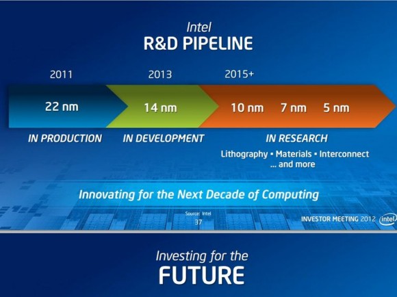
Exploiting the latter benefit, we have the realization above. By 2020, which assuming a 2 year cadence between process nodes means we're talking about silicon built on a 5nm process, Intel expects that the size of "meaningful compute" approaches zero. It's not totally clear what Intel defines as meaningful compute, but if you keep in mind that a single AMD Jaguar core measures < 3mm^2 at 28nm, it's not a stretch to believe that we'd have quite a bit of compute available nearly for free at 5nm. Assuming perfect scaling (not going to happen), a 100mm^2 die at 22nm would measure only 6.25mm^2 at 5nm. Even if you don't get perfect scaling, Moore's Law can give us the performance we get in a smartphone today in a size that's small enough and cheap enough to make that we can integrate it anywhere (smart-tables anyone?).
The idea of ubiquitous compute has been around for quite a while, but it's still mindblowing to think about what can happen once meaningful compute is really almost free. Remember that there's a direct relationship between the size of silicon and its cost. Today's 80 - 120mm^2 smartphone SoCs cost anywhere from $10 - $30 to integrate into a phone. If silicon with that level of complexity can be reduced in size to the point where we're looking at low single digit costs, the potential impact to new markets will be huge.
We saw what affordable compute did for smartphones, the next question is what even more affordable compute can do for other, undiscovered markets. A while ago I heard someone smart tell me that at some point displays become cheap enough where many surfaces we take for granted, start integrating them (e.g. bathroom mirrors that double as displays). Combine that with cheap compute that we can integrate everywhere as well and we have a recipe for the future.


37 Comments
View All Comments
Sothryn - Tuesday, September 11, 2012 - link
Using the example from the article "100mm^2 die at 22nm would measure only 6.25mm^2 at 5nm"nm die size
22 100
14 50
10 25
7 12.5
5 6.25
Each generation is half the die size of the previous generation. So, despite the nm value seeming to slow, the die size shrinkage continues at a staggering rate.
Sothryn - Tuesday, September 11, 2012 - link
Never trust formatting:nm .....die size in mm^2
22 ......100
14 ........50
10 ........25
..7 ........12.5
..5 ...........6.25
jjj - Monday, September 10, 2012 - link
Except you are looking at the wrong thing,the math for die size is not relevant since power consumption doesn't scale with it.And afterall meaningful compuute is not all that meaningful in a connected device.
Kevin G - Monday, September 10, 2012 - link
Power consumption doesn't scale down by the same rate but it does scale down if ever so slightly by raw process technology.The other thing to look as is interconnects and the associated power consumption to go off die. Say at 7 nm a manufacturer can integrate a full 1 GB of eDRAM on a reasonably sized die, that significantly reduces power consumption compared to have 1 GB of RAM in an external package.
There has also been research into near threshold voltage for operation. Intel's current experiments into this have yielded a Pentium class device running as low as 2 milliwatt running off of a solar cell. If you can run it off of solar with enough energy to spare to recharge a small battery, you may never even need to be connected to start.
uibo - Monday, September 10, 2012 - link
A while back NVIDIA posted some slides about "nvidia-deeply-unhappy-with-tsmc-claims-22nm-essentially-worthless", where it projected that starting from 28nm the gains in price from shrinking are nearing zero. The development of these new processes is so complex and expensive, that the big guys are forced to collaborate more in their research.In 2010, an Australian team announced that they fabricated a single functional transistor out of 7 atoms that measured 4 nm in length.
Being so close to the limit, I am pretty sure everybody is going to drag this out for as long as possible.
DanNeely - Monday, September 10, 2012 - link
The smaller fabs might want to drag it out; but Chipzilla is unlikely to stop throwing billions into R&D to maintain it's ~1 year process lead over the competition; being able to expand their lead to 2 or 3 years would make them jump for joy. Avoiding falling even farther behind means that Global Foundries/TSMC/Samsung/IBM can't stall even if they want to.drmrking - Monday, September 10, 2012 - link
last years AMD conf had a presentation from ARM that basically explained the issue going forward was not about die shrinkage but how to dissipate heat and manage power. shrinking the die does not get you more performance per sqmm because you can't dissipate the heat fast enough. Best they said we could hope for was a bunch of different functionality silicon that was switched on and off as needed, but the power sloshing was a real challenge. Fascinating presentation. Mike.Mr Perfect - Tuesday, September 11, 2012 - link
I vaguely recall that, it was their "dark silicon" presentation, right? They said that while today's chips dissipate heat quickly enough to have the whole die active at once, future processes would have to power gate increasingly large sections of the die to keep thermals in check.bobbozzo - Monday, September 10, 2012 - link
s/prefect/perfect/1008anan - Monday, September 10, 2012 - link
Anand,The way I prefer to think about this is in terms of single precision gigaflops per TDP watt and double precision gigaflops per watt (for HPC, servers and desktops).
Could you share your own perspectives on how fast single precision gigaflops per watt will grow over time?
Right now the fastest GPGPU accelerator is 20 single precision gigaflops per watt, with smarphone SoCs running in the 2 to 8 gigaflops per watt range. What gigaflops per watt do you see with 20 nm, 14 nm, 10 nm for the ARM ecosystem and what gigaflops per watt do you see for Atom N, Atom Z, 10 watt TDP Haswell at 22 nm; for Intel at 14 nm, for Intel at 10 nm, 7 nm etc.