NVIDIA GeForce GTX 680 Review: Retaking The Performance Crown
by Ryan Smith on March 22, 2012 9:00 AM ESTMeet the GeForce GTX 680
All things considered the design of the GeForce GTX 680 is not a radical departure from the GTX 580, but at the same time it also has some distinct differences owing to the fact that its TDP is some 50W lower than GTX 580.
Like the past GTX x80 cards, the basic design of the GTX 680 is that of a blower. A radial fan at the rear of the card sucks in air and pushes it towards the front of the card. Notably, due to a combination of card length and the fan position, the “wedge” around the fan has been done away with. NVIDIA tells us that this shouldn’t significantly impact the cooling of the card, particularly since it has a lower TDP in the first place, but when used in SLI it will remove some of the breathing room than the GTX 580 enjoyed.
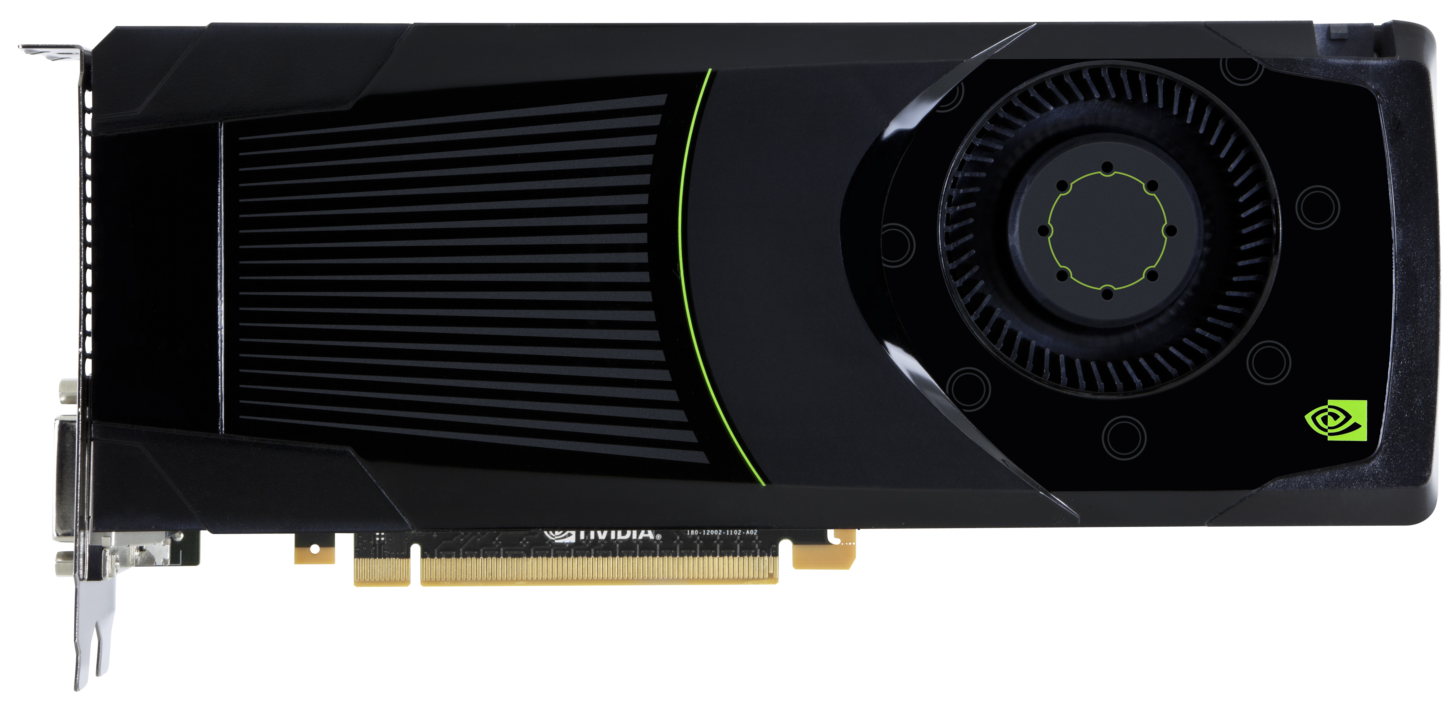
Looking at the fan itself, compared to the GTX 580 the fan has been moved from the center of the card to the top of the card. This is due to NVIDIA’s port configuration, which uses a stacked DVI connector that consumes what would have normally been part of the exhaust vent on the GTX 580. We’ll get into the port configuration more in a minute, but for the moment the significance is that because the GTX 680 only has half a vent NVIDIA has moved the fan to match the vent, which is why the fan has been moved up.
On that note, the repositioning of the fan also had its own ramifications. Because the fan is now so close to the top and at the same time so close to the rear, NVIDIA went with a unique method of arranging the PCIe power sockets. Rather than having them side-by-side as we’ve seen on countless NVIDIA cards in the past, the sockets are stacked on each other in a staggered configuration. With the fan otherwise occupying the space that one of the sockets would take up, this configuration allowed NVIDIA to have two sockets without lengthening the card just to fit another socket. Overall this staggered design is not too difficult to work with, though with one socket facing the opposite way it might require some cable repositioning if you have a well maintained cable run.
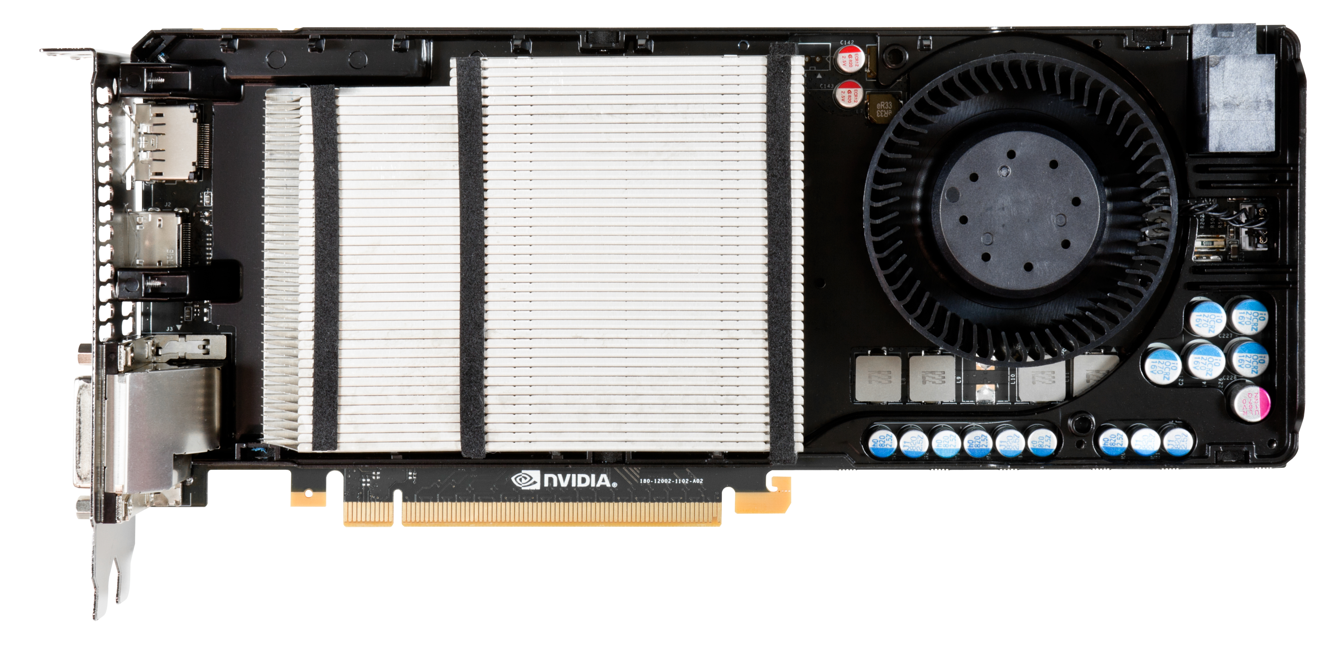
Moving on, when we remove the shroud on the GTX 680 we see the fan, baseplate, and heatsink in full detail. NVIDIA is using an aluminum fin stacked heatsink, very similar to what we saw on the GTX 580. Underneath the heatsink NVIDIA is using a set of three heatpipes to transfer heat between the GPU and the heatsink. This is as opposed to the vapor chamber on the GTX 580, and while this setup doesn’t allow empirical testing, given the high efficiency of vapor chambers it’s likely that this isn’t quite as efficient, though to what degree we couldn’t say.
Finally, after removing the fan, baseplate, and heatsink, we can see the PCB in full detail. Unlike GF110 and GF114, GK104 is not capped with an IHS, allowing for the heatsink to directly come in contact with the GPU die. Meanwhile arranged around the GPU we can see the 8 2Gb GDDR5 RAM modules that give the GTX 680 its 2GB of RAM. These are Hynix R0C modules, which means they’re rated for 6GHz, the stock memory speed for the GTX 680. Overall the card measures 10” long with no overhang from the shroud, making it 0.5” shorter than the GTX 580.
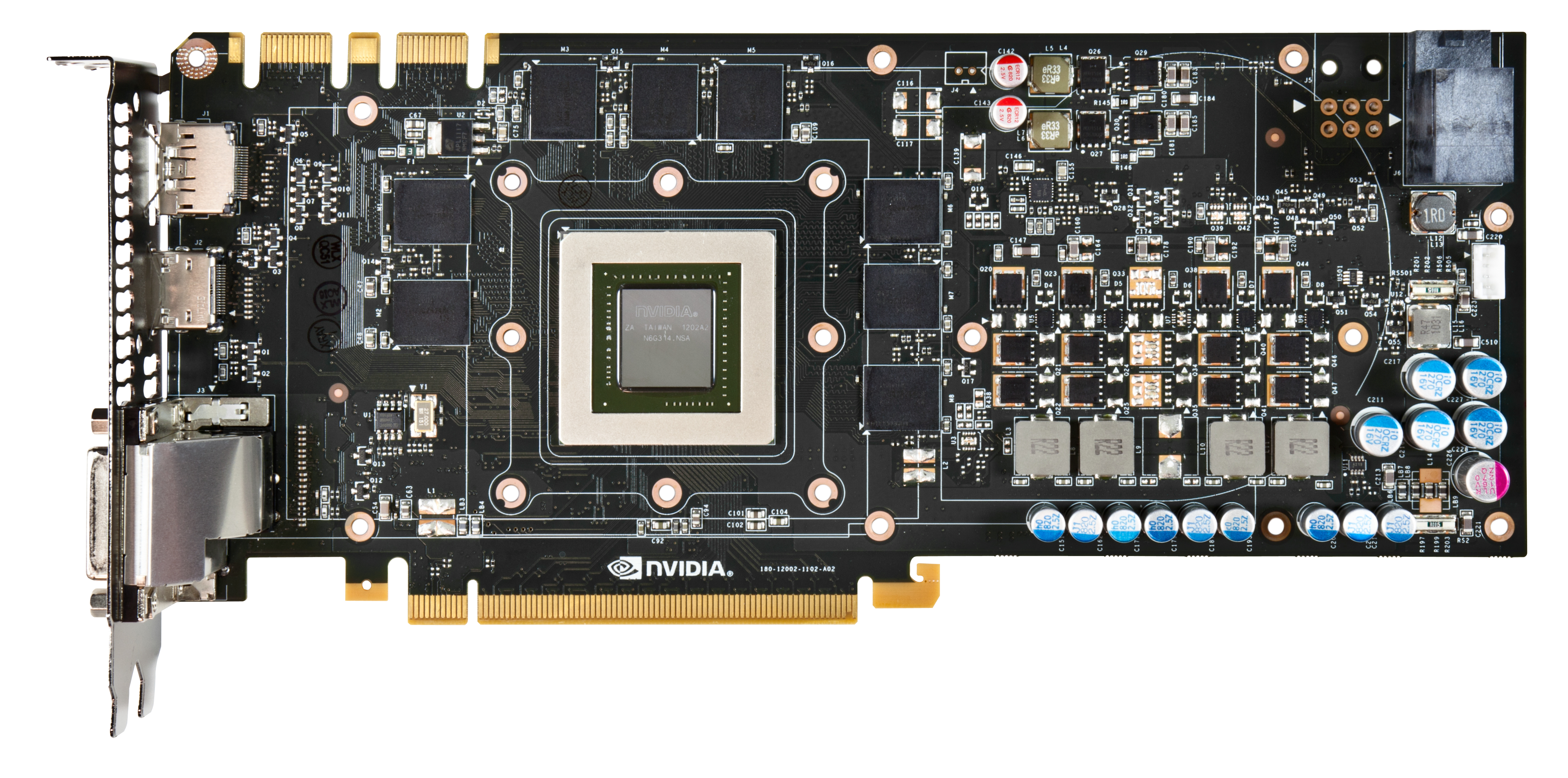
Looking at the top of the card, as always we see the SLI connectors. Following in the footsteps of the GTX 580, the GTX 680 features 2 SLI connectors, allowing for up to 3-way SLI.
Meanwhile at the front of the card we see the I/O bracket. As we alluded to previously, the GTX 680 uses a stacked DVI design here; NVIDIA has done everything they can to keep the DVI ports at the very bottom of the card to avoid impeding airflow, but the upper DVI port still occupies roughly 40% of what would otherwise be the vent. Altogether the GTX 680 features 2 DL-DVI ports, a full size HDMI port, and a full size DisplayPort.
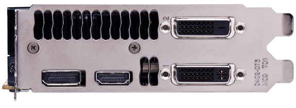
While NVIDIA has used DVI and HDMI ports for quite some time, this is the first time NVIDIA has included DIsplayPort on a reference design. Unfortunately we find that this ruffles our feathers a bit, although this isn’t strictly NVIDIA’s fault. As we’ve covered in the past, DisplayPort comes in both a full size and miniDP configuration – AMD in particular has used miniDP since the Radeon HD 6800 series in 2010. And while we’re happy to see DisplayPort finally make it into an NVIDIA reference design, the fact that it’s a full size DisplayPort is less than encouraging because at this point in time DisplayPort has largely been replaced by miniDP.
Ultimately the fault for this lies more with the VESA than NVIDIA, but it’s indicative of a larger problem in the DisplayPort community in that both full size DP and miniDP are equally valid and equally capable ports. While full size DisplayPort has the distinction of coming first, thanks in large part to Apple it has largely been displaced by miniDP as the most common variant on source devices. The problem with this is that both miniDP and DisplayPort are now in wide use; wide, redundant use.
At this point desktop computers and video cards coming with full size DisplayPorts is silly at best, and frustrating at worst. The laptop guys aren’t going to give up miniDP due to the space savings, and there’s no significantly good reason to use DisplayPort on desktops when miniDP offers the same functionality. We would rather see the PC industry standardize on miniDP across all source devices, and thereby eliminate any ambiguity with regards to what cables or adaptors are necessary. DisplayPort adoption has been slow enough – having 2 variants of the port on source devices only makes it more confusing for everyone.
Finally, while we’re on the subject of display connectivity we quickly took a look at how the idle clockspeeds of GTX 680 are impacted by the use of multiple displays. With 2 displays GTX 680 can utilize its full idle clocks, but only if both displays are connected via a TMDS type connection (DVI/HDMI) and run with identical timings. But if different timings are used or if one display is connected via DisplayPort, then the GTX 680 will shift to its low power 3D clocks. However if we expand that to 3 monitors and enable NVIDIA Surround, then the GTX 680 can operate at full idle regardless of whether DisplayPort is used or not.


404 Comments
View All Comments
chizow - Thursday, March 22, 2012 - link
Nvidia let AMD off the hook by productizing a mid-range GK104 ASIC as their flagship SKU and pricing it at $500.Its a great part no doubt and beats AMD in every metric, but as the article stated, its still going to be the smallest increase in price:performance that we've seen since 9800GTX.
Overall 28nm has been a huge disappointment so far in terms of performance increase over previous generations at the same price points, I guess we will have to wait for 28nm BigK to get that true high-end increase you'd expect from a smaller process node and new GPU arch.
B-Unit1701 - Thursday, March 22, 2012 - link
'Off the hook'? LMAO they released what they had. They are already months late, the only other option would have been to just not release a card this generation, would THAT have made you happier?chizow - Thursday, March 22, 2012 - link
No, what would have made me happier from both Nvidia and AMD would be to follow their own historical price:performance metrics.Instead, we have AMD first trying to pass an overall unimpressive Tahiti part as a high-end flagship at $550+ followed by Nvidia following suit by pricing their mid-range ASIC as a $500 part.
28nm has been a big disappointment so far, as we have the smallest increase in price:performance in any generation or process shrink since the 9800GTX.
CeriseCogburn - Thursday, March 22, 2012 - link
With AMD GF foundry failures TSMC is stoked to the gills. We're not going to get the prices you want for performance for another 6 months or so when production is freed up with TSMC's ongoing 2B expansion.You ought to include real inflation as well which is as we all know far higher than the socialist government figures that are suppressed so their automatic payout increases are lessened.
Be disappointed, a valid point, there are extenuating factors.
xrror - Thursday, March 22, 2012 - link
exactly. I completely understand why Nvidia is charging $500 for their mid-range part, but it still sucks.AMD also... I get why the 6000 series was gimped (it was originally supposed to be 32nm, and that fell through) but 7000 series... maybe that can be explained by moving to a new arch with GCN.
Regardless... disappointing. Well actually it's dissapointing that you must pay $500+ to get a card that /might/ give you a fresh gaming experience over the $350 card you bought last generation.
Unless AMD can pull a 8000 gen card out of their arse with drivers that work (i'm not optimistic) then you can bet if/when "full Kepler" comes out it will be $800+
CeriseCogburn - Friday, March 23, 2012 - link
Charlie D with his $299 leak, the only source, has made everyone think the 1core top card in the world was going to be released $150 cheaper than the current top 1core card in the world.He must still be laughing hard at semi-accurate.
chizow - Friday, March 23, 2012 - link
It wasn't Charlie's leak, it was the combined evidence of ~300mm^2 size, transistor count, mid-range specs, ASIC designation, and leaked GTX 670Ti pics also leading people to the conclusion this part was originally meant to be priced in that $250-$350 range.Obviously GK104 performed better than expected, coupled with Tahiti being weaker than expected, resulting in what we see today: an exceptionally performing mid-range ASIC being SKU'd as an overpriced flagship part at premium pricing.
CeriseCogburn - Tuesday, March 27, 2012 - link
Sorry I don't buy any of it. It's a "new architecture", if we take Charlie's leak, everything fits but the price, and every price has been $499 going on 4X in a row at least.chizow - Friday, March 23, 2012 - link
I agree, but honestly I don't even think AMD can compete at this point. Nvidia has beaten AMD at its own game soundly (small die, power efficient strategy, and done it with their 2nd best ASIC.Now they're free to make the slightly faster, power-hungry GPGPU monster GPU with as much TDP as they like without having to hear about it being worst than AMD's tree-hugging specs.
Sabresiberian - Friday, March 23, 2012 - link
Nvidia releasing their new architecture a few months after AMD released theirs does not make them late. Nvidia's schedule hasn't been the same as AMD's for several years now.And, what's AMD's answer to Big Kepler going to be? They lost today to Nvidia's mid-line chip, they will lose big time when Big Kepler comes out. By the time they catch up, Maxwell will be breathing down their necks.
;)