NVIDIA's Tegra 3 Launched: Architecture Revealed
by Anand Lal Shimpi on November 9, 2011 12:34 AM ESTOriginally announced in February of this year at MWC, NVIDIA is finally officially launching its next-generation SoC. Previously known under the code name Kal-El, the official name is Tegra 3 and we'll see it in at least one product before the end of the year.
Like Tegra 2 before it, NVIDIA's Tegra 3 is an SoC aimed at both smartphones and tablets built on TSMC's 40nm LPG process. Die size has almost doubled from 49mm^2 to somewhere in the 80mm^2 range.

The Tegra 3 design is unique in the industry as it is the first to implement four ARM Cortex A9s onto a chip aimed at the bulk of the high end Android market. NVIDIA's competitors have focused on ramping up the performance of their dual-core solutions either through higher clocks (Samsung Exynos) or through higher performing microarchitectures (Qualcomm Krait, ARM Cortex A15). While other companies have announced quad-core ARM based solutions, Tegra 3 will likely be the first (and only) to ship in an Android tablet and smartphone in 2011 - 2012.
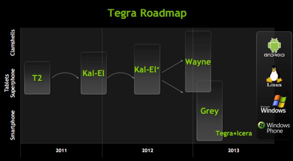
NVIDIA will eventually focus on improving per-core performance with subsequent iterations of the Tegra family (perhaps starting with Wayne in 2013), but until then Tegra 3 attempts to increase performance by exploiting thread level parallelism in Android.
GPU performance also sees a boon thanks to a larger and more efficient GPU in Tegra 3, but first let's talk about the CPU.
Tegra 3's Four Five Cores
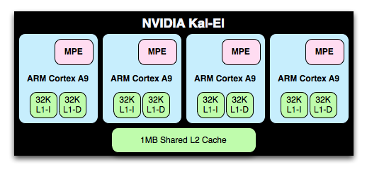
The Cortex A9 implementation in Tegra 3 is an improvement over Tegra 2; each core now includes full NEON support via an ARM MPE (Media Processing Engine). Tegra 2 lacked any support for NEON instructions in order to keep die size small.
NVIDIA's Tegra 2 die
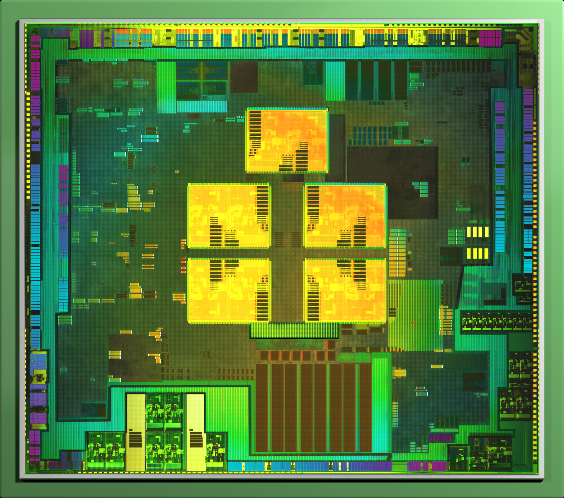
NVIDIA's Tegra 3 die, A9 cores highlighted in yellow
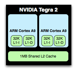
L1 and L2 cache sizes remain unchanged. Each core has a 32KB/32KB L1 and all four share a 1MB L2 cache. Doubling core count over Tegra 2 without a corresponding increase in L2 cache size is a bit troubling, but it does indicate that NVIDIA doesn't expect the majority of use cases to saturate all four cores. L2 cache latency is 2 cycles faster on Tegra 3 than 2, while L1 cache latencies haven't changed. NVIDIA isn't commenting on L2 frequencies at this point.
The A9s in Tegra 3 can run at a higher max frequency than those in Tegra 2. With 1 core active, the max clock is 1.4GHz (up from 1.0GHz in the original Tegra 2 SoC). With more than one core active however the max clock is 1.3GHz. Each core can be power gated in Tegra 3, which wasn't the case in Tegra 2. This should allow for lightly threaded workloads to execute on Tegra 3 in the same power envelope as Tegra 2. It's only in those applications that fully utilize more than two cores that you'll see Tegra 3 drawing more power than its predecessor.
The increase in clock speed and the integration of MPE should improve performance a bit over Tegra 2 based designs, but obviously the real hope for performance improvement comes from using four of Tegra 3's cores. Android is already well threaded so we should see gains in portions of things like web page rendering.
It's an interesting situation that NVIDIA finds itself in. Tegra 3 will show its biggest performance advantage in applications that can utilize all four cores, yet it will be most power efficient in applications that use as few cores as possible.
There's of course a fifth Cortex A9 on Tegra 3, limited to a maximum clock speed of 500MHz and built using LP transistors like the rest of the chip (and unlike the four-core A9 cluster). NVIDIA intends for this companion core to be used for the processing of background tasks, for example when your phone is locked and in your pocket. In light use cases where the companion core is active, the four high performance A9s will be power gated and overall power consumption should be tangibly lower than Tegra 2.
Despite Tegra 3 featuring a total of five Cortex A9 cores, only four can be active at one time. Furthermore, the companion core cannot be active alongside any of the high performance A9s. Either the companion core is enabled and the quad-core cluster disabled or the opposite.
NVIDIA handles all of the core juggling through its own firmware. Depending on the level of performance Android requests, NVIDIA will either enable the companion core or one or more of the four remaining A9s. The transition should be seamless to the OS and as all of the cores are equally capable, any apps you're running shouldn't know the difference between them.


94 Comments
View All Comments
psychobriggsy - Friday, November 11, 2011 - link
In the Android market, it really doesn't matter what features Apple includes in their in-house SoC for their iOS devices.Considering that manufacturers are having problems fabbing larger high-DPI displays, I also wouldn't be betting on the iPad 3 having a higher resolution display. And Apple would go for 2048x1536 for simplicities sake.
Five months is also a long time in the ARM SoC market, one that NVIDIA will try to make use of. Let's just hope the product meets the hype when reviews roll in.
name99 - Wednesday, November 9, 2011 - link
I've asked this before, and I will ask it again:What software on Android, shipping TODAY, is capable of using 4 cores usefully?
The browser? The PDF viewer? Google Earth? If so, they're all ahead of their desktop cousins.
Yes, yes, people are buying the future. And, sure, one day, software will be revved to use 4 cores. (But, this being Android, chances are, the particular device you buy this year using Tegra3 will NOT be revved.)
I'm not trying to be snarky here, just realistic. It seems to me the competitors ARM manufacturers are targeting the real world, where dual cores can (to some extent) usefully be used. But nVidia is requiring people who adopt this chip to pay for power that, realistically, they're not going to use. This seems a foolish design choice. It seems to me far more sensible for mobile to basically track (lagging by about a year) desktop. Desktop is seeing quad-core adoption in a few places, but it's hardly mainstream --- and I'd say that until, let's say, the low-end MacBook Air is using quad core, that's an indication that "software" (as a general class) probably hasn't been threaded enough to make quad-core worth-while in mobile.
Yes, it's harder, but until then, I'd say far more useful to look at what's ACTUALLY causing people slowness and hassle on phones and tablets, and add THAT to your chips. So, faster single-threaded core --- great. But think more generally.
Flash on these devices is still slow. Could you speed it up somehow --- maybe a compression engine to transparently compress data sent to/from flash? Likewise app launch is slow. Are there instructions that could be added to speed up dynamic linking? Memory is a problem, and again transparent compression might be helpful there.
Basically --- solve the problems people actually have, even if they are hard, NOT the problems you wish people had because you know how to solve those.
psychobriggsy - Friday, November 11, 2011 - link
The video shows web browsing and games to be using three cores quite often, and the fourth quite a bit. Android is quite multi-threaded, and if it also supports the Java Concurrency APIs it is very easy for software to also be multi-threaded.I also presume that the GeForce drivers and other Tegra SoC drivers utilise multi-threading as much as possible.
And Flash is being dropped on mobile devices in favour of HTML5. That's Adobe making that move. And not before time, it is a horrible technology.
Romulous - Thursday, November 10, 2011 - link
Meh. There may come a time when cores dont metter much.http://www.euclideon.com/ :)
alphadon - Thursday, November 10, 2011 - link
"Die size has almost doubled from 49mm^2 to somewhere in the 80mm^2 range"49^2 = 2401
80^2 = 6400
This should probably read:
"Die size has bloated to over 2.5 times the area of the prior generation leaving everyone wondering why NVIDIA is releasing this 40nm dinosaur. We would have expected a die shrink to keep the power and space requirements in line with the industry's competitors, but seeing all that real estate squandered on such an evolutionary product is downright shameful."
Lugaidster - Friday, November 11, 2011 - link
Did you even read the other posts? The other competitors have bigger dies and less cores! and also, the geometry didn't change between tegra 2 and this.I find it great that they were able to double the shader core count, increase core count from 2 to 5 (it's slower but not less complex, see the die picture) and increase frequency while still having a smaller die than the competition.
I think that given the constraints, this might turn out to be a good product. Obviously only time will tell if it actually performs, but who knows...
Lugaidster - Friday, November 11, 2011 - link
By the way, its 49 mm² not 49² mm. So its actually less than twice as big.psychobriggsy - Friday, November 11, 2011 - link
Do you seriously think the Tegra 3 die size is 8cm by 8cm?49mm^2 is the area, not the edge dimension. In effect the die size has gone from around 7mm x 7mm to 9mm x 9mm. I.e., your little finger nail to your index finger nail (your hands may vary).
psychobriggsy - Friday, November 11, 2011 - link
In addition the 28nm shrink of Tegra 3 (Tegra 3+) next year, if no extra features are added, will shrink the die from 80mm^2 to 40mm^2 (in an ideal world, let's say 50mm^2 worst case and shrinks aren't simple). And Tegra 4 will probably be around 80-100 mm^2 again.lightshapers - Friday, November 11, 2011 - link
This quad core architecture is still disappointing. Actually they implemented a 4th core with good reinforcement from marketing, presented to be a solution for low power consumption at low CPU load. My guess is actually all competitors can do this (cut clocks and power on all but one CPU and reduce cluster frequency) on the ARM dual cluster without the need to add an extra CPU ( I speak for Samsung and TI, as Qualcomm is designing their own). In addition to that, this 5th core is another non negligible additional gates that leak.Then, the action to synchronize L2 Cache by arm coherency port is fast, but 1MB is 1MB, which means probably few hundreds of us for lost reactivity when switching between cluster and this 5th core.
And at the end, it doesn't really solve all the problems of having 4 cores, as asymmetry in core load balance will ever happen. This solution may solve the low load case. But over the low-load watermark, the cluster is power-up, and we have 4 core consuming at least their leakage. This was reported as an issue on tegra2, I don't think it has changed (the 5th is in some way the proof), but here we have 2 additional cores...
For example, medium load requires 2 cores. 5th is off, but consumption is 4 times the consumption of one.
It would have been smarter to design a full speed additional core, so as to get a higher "low limit load" so as to stay on 1st core as longer as possible. With 500Mhz, it's difficult to say if you can manage all graphical interface + OS background on a 720p device...