NVIDIA's Tegra 3 Launched: Architecture Revealed
by Anand Lal Shimpi on November 9, 2011 12:34 AM ESTOriginally announced in February of this year at MWC, NVIDIA is finally officially launching its next-generation SoC. Previously known under the code name Kal-El, the official name is Tegra 3 and we'll see it in at least one product before the end of the year.
Like Tegra 2 before it, NVIDIA's Tegra 3 is an SoC aimed at both smartphones and tablets built on TSMC's 40nm LPG process. Die size has almost doubled from 49mm^2 to somewhere in the 80mm^2 range.

The Tegra 3 design is unique in the industry as it is the first to implement four ARM Cortex A9s onto a chip aimed at the bulk of the high end Android market. NVIDIA's competitors have focused on ramping up the performance of their dual-core solutions either through higher clocks (Samsung Exynos) or through higher performing microarchitectures (Qualcomm Krait, ARM Cortex A15). While other companies have announced quad-core ARM based solutions, Tegra 3 will likely be the first (and only) to ship in an Android tablet and smartphone in 2011 - 2012.
NVIDIA will eventually focus on improving per-core performance with subsequent iterations of the Tegra family (perhaps starting with Wayne in 2013), but until then Tegra 3 attempts to increase performance by exploiting thread level parallelism in Android.
GPU performance also sees a boon thanks to a larger and more efficient GPU in Tegra 3, but first let's talk about the CPU.
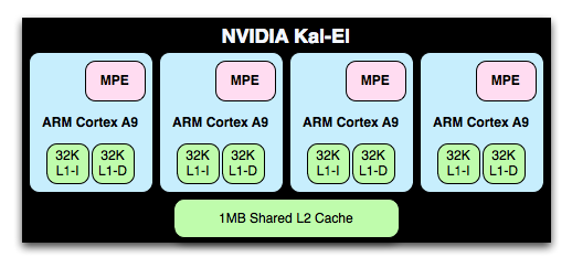
Tegra 3's Four Five Cores
The Cortex A9 implementation in Tegra 3 is an improvement over Tegra 2; each core now includes full NEON support via an ARM MPE (Media Processing Engine). Tegra 2 lacked any support for NEON instructions in order to keep die size small.
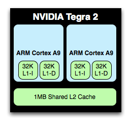
NVIDIA's Tegra 2 die
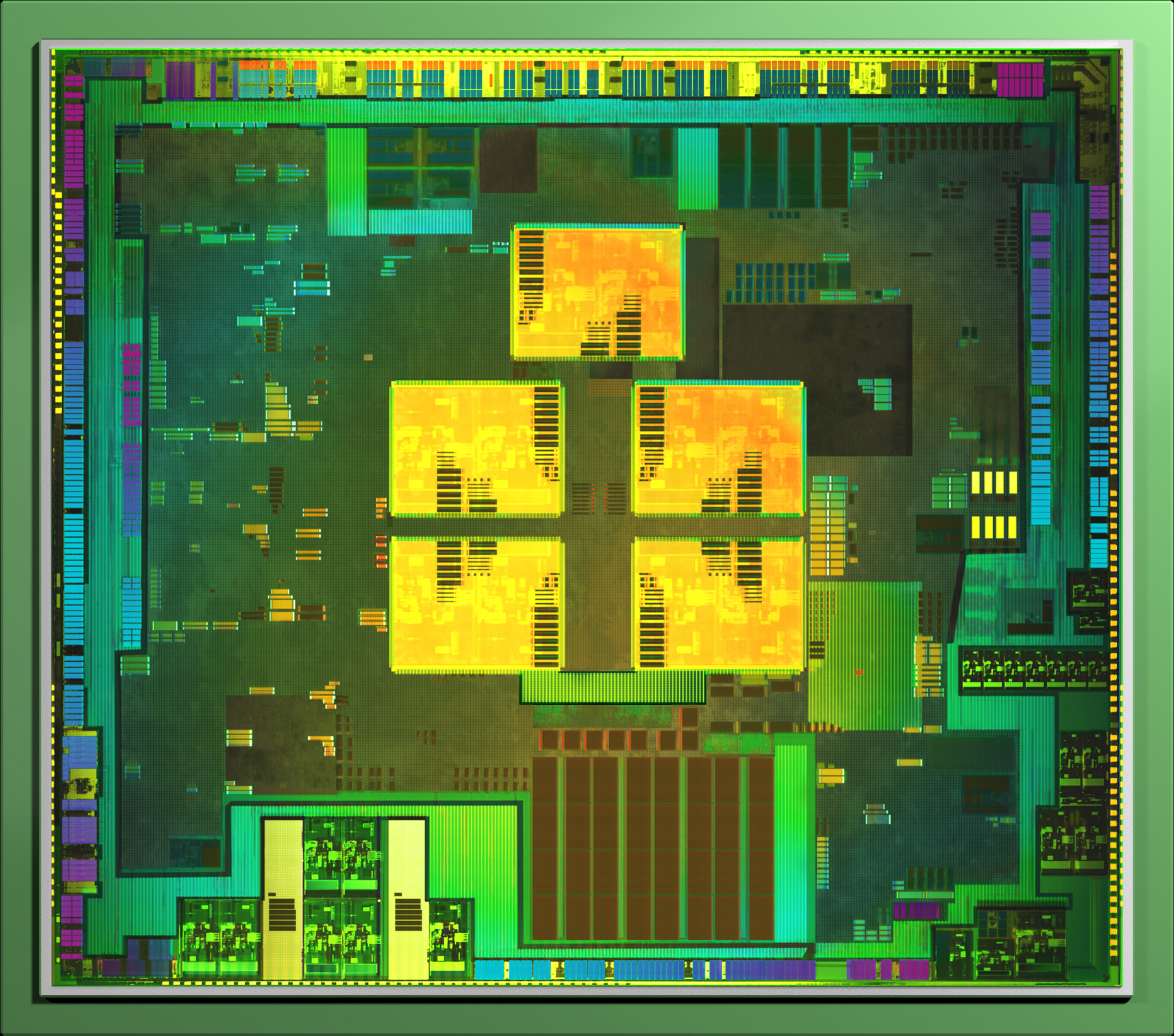
NVIDIA's Tegra 3 die, A9 cores highlighted in yellow
L1 and L2 cache sizes remain unchanged. Each core has a 32KB/32KB L1 and all four share a 1MB L2 cache. Doubling core count over Tegra 2 without a corresponding increase in L2 cache size is a bit troubling, but it does indicate that NVIDIA doesn't expect the majority of use cases to saturate all four cores. L2 cache latency is 2 cycles faster on Tegra 3 than 2, while L1 cache latencies haven't changed. NVIDIA isn't commenting on L2 frequencies at this point.
The A9s in Tegra 3 can run at a higher max frequency than those in Tegra 2. With 1 core active, the max clock is 1.4GHz (up from 1.0GHz in the original Tegra 2 SoC). With more than one core active however the max clock is 1.3GHz. Each core can be power gated in Tegra 3, which wasn't the case in Tegra 2. This should allow for lightly threaded workloads to execute on Tegra 3 in the same power envelope as Tegra 2. It's only in those applications that fully utilize more than two cores that you'll see Tegra 3 drawing more power than its predecessor.
The increase in clock speed and the integration of MPE should improve performance a bit over Tegra 2 based designs, but obviously the real hope for performance improvement comes from using four of Tegra 3's cores. Android is already well threaded so we should see gains in portions of things like web page rendering.
It's an interesting situation that NVIDIA finds itself in. Tegra 3 will show its biggest performance advantage in applications that can utilize all four cores, yet it will be most power efficient in applications that use as few cores as possible.
There's of course a fifth Cortex A9 on Tegra 3, limited to a maximum clock speed of 500MHz and built using LP transistors like the rest of the chip (and unlike the four-core A9 cluster). NVIDIA intends for this companion core to be used for the processing of background tasks, for example when your phone is locked and in your pocket. In light use cases where the companion core is active, the four high performance A9s will be power gated and overall power consumption should be tangibly lower than Tegra 2.
Despite Tegra 3 featuring a total of five Cortex A9 cores, only four can be active at one time. Furthermore, the companion core cannot be active alongside any of the high performance A9s. Either the companion core is enabled and the quad-core cluster disabled or the opposite.
NVIDIA handles all of the core juggling through its own firmware. Depending on the level of performance Android requests, NVIDIA will either enable the companion core or one or more of the four remaining A9s. The transition should be seamless to the OS and as all of the cores are equally capable, any apps you're running shouldn't know the difference between them.


94 Comments
View All Comments
Itaintrite - Wednesday, November 9, 2011 - link
That HD decode processor will make a lot of people happy.JoeTF - Thursday, November 10, 2011 - link
No it bloody won't. Tegra2 already has hardware video decode unit and it's main trademark is that, it cannot even decode properly (no prediction, but more importantly - not enough power to decode anything higher than L3.0 at 30fps).Hardware video decoder in Tegra3 is pretty much unchanged from T2. Hell, you can see light framedrops even in their marketing video.
Good thing is that they added NEON instruction. Sadly, it mean we will have to use all four cores at 100% utilization to playback our videos correctly and under those conditions runtime will be severely constrained (the 8h they talk about is for hardware decode, not NEON-based cpu decode)
3DoubleD - Thursday, November 10, 2011 - link
This is what I've been holding out for, so I really hope your wrong.psychobriggsy - Friday, November 11, 2011 - link
The article states that the video decoder has been significantly enhanced in Tegra 3. Where do you get your information from?Jambe - Wednesday, November 9, 2011 - link
"Die size has almost doubled from 49mm^2 to somewhere in the 80mm^2 range."~80mm^2 is considerably more than double the area of 49mm^2, isn't it?
eddman - Wednesday, November 9, 2011 - link
Umm, no!! 80 is 63% bigger than 49. Simple as that.MamiyaOtaru - Friday, November 11, 2011 - link
c'mon man it's not 49 millimeters squared, its 49 square millimeters. 49/80 is well less than 1/2MamiyaOtaru - Friday, November 11, 2011 - link
see this for some review: http://img379.imageshack.us/img379/6015/squaremmhe...vision33r - Wednesday, November 9, 2011 - link
The Tegra 3 by being evolutionary, left a huge opening for other SOC to surpass it in a matter of months.I don't think the performance will be that huge like the Apple A4 - A5 is on the magnitude of 9x faster.
It will be worthless by April when the Apple A6 comes out and spanks it silly and rumor has it that Apple maybe using a 1600x1200 10" display to up the ante.
If this is true, it means Nvidia has to bring out a Tegra 4 fall summer or fall 2012.
It will be a big iPad 2 X-mas for sure and iPad 3 will easily trump Tegra 3.
metafor - Wednesday, November 9, 2011 - link
I honestly don't think the biggest decision-maker for people considering an iOS tablet or Android tablet has to do with a ~40% difference in GPU performance.When comparing Android tablets to each other -- since the OS is the same -- many people will fall back on "well, x is faster than y". But a 2x performance difference isn't going to change my mind if I like Android better than iOS, or vice versa.
Things like a high-res screen, battery life and usability of the OS have a much bigger impact; so I'd say nVidia or really any Android SoC vendor really aren't competing with Apple's silicon group.