Kal-El Has Five Cores, Not Four: NVIDIA Reveals the Companion Core
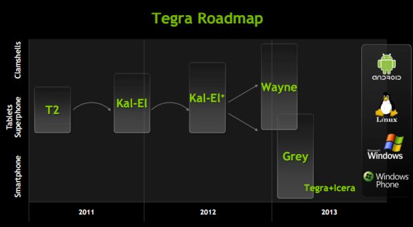
by Anand Lal Shimpi on September 20, 2011 11:46 AM ESTLast week NVIDIA provided an update on its Tegra SoC roadmap. Kal-El, its third generation SoC (likely to launch as Tegra 3) has been delayed by a couple of months. NVIDIA originally expected the first Kal-El tablets would arrive in August, but now it's looking like sometime in Q4. Kal-El's successor, Wayne, has also been pushed back until late 2012/early 2013. In between these two SoCs is a new part dubbed Kal-El+. It's unclear if Kal-El+ will be a process shrink or just higher clocks/larger die on 40nm.
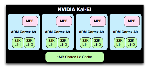
In the smartphone spirit, NVIDIA is letting small tidbits of information out about Kal-El as it gets closer to launch. In February we learned Kal-El would be NVIDIA's first quad-core SoC design, featuring four ARM Cortex A9s (with MPE) behind a 1MB shared L2 cache. Kal-El's GPU would also see a boost to 12 "cores" (up from 8 in Tegra 2), but through architectural improvements would deliver up to 3x the GPU performance of T2. Unfortunately the increase in GPU size and CPU core count doesn't come with a wider memory bus. Kal-El is still stuck with a single 32-bit LPDDR2 memory interface, although max supported data rate increases to 800MHz.
We also learned that NVIDIA was targeting somewhere around an 80mm^2 die, more than 60% bigger than Tegra 2 but over 30% smaller than the A5 in Apple's iPad 2. NVIDIA told us that although the iPad 2 made it easier for it to sell a big SoC to OEMs, it's still not all that easy to convince manufacturers to spend more on a big SoC.
Clock speeds are up in the air but NVIDIA is expecting Kal-El to run faster than Tegra 2. Based on competing A9 designs, I'd expect Kal-El to launch somewhere around 1.3 - 1.4GHz.
Now for the new information. Power consumption was a major concern with the move to Kal-El but NVIDIA addressed that by allowing each A9 in the SoC to be power gated when idle. When a core is power gated it is effectively off, burning no dynamic power and leaking very little. Tegra 2 by comparison couldn't power gate individual cores, only the entire CPU island itself.
In lightly threaded situations where you aren't using all of Kal-El's cores, the idle ones should simply shut off (if NVIDIA has done its power management properly of course). Kal-El is built on the same 40nm process as Tegra 2, so when doing the same amount of work the quad-core chip shouldn't consume any more power.
Power gating idle cores allows Kal-El to increase frequency to remaining active cores resulting in turbo boost-like operation (e.g. 4-cores active at 1.2GHz or 2-cores at 1.5GHz, these are hypothetical numbers of course). Again, NVIDIA isn't talking about final clocks for Kal-El or dynamic frequency ranges.
Five Cores, Not Four
Courtesy NVIDIA
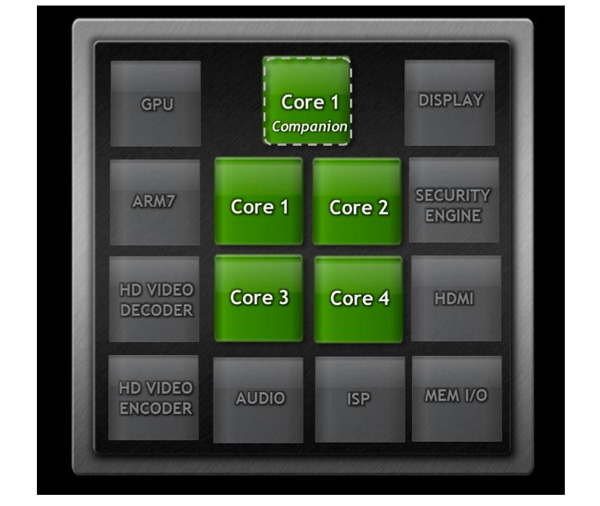
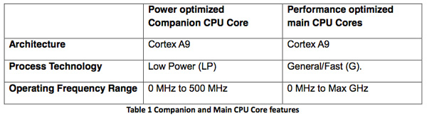
Finally we get to the big news. There are actually five ARM Cortex A9s with MPE on a single Kal-El die: four built using TSMC's 40nm general purpose (G) process and one on 40nm low power (LP). If you remember back to our Tegra 2 review you'll know that T2 was built using a similar combination of transistors; G for the CPU cores and LP for the GPU and everything else. LP transistors have very low leakage but can't run at super high frequencies, G transistors on the other hand are leaky but can switch very fast. Update: To clarify, TSMC offers a 40nm LPG process that allows for an island of G transistors in a sea of LP transistors. This is what NVIDIA appears to be using in Kal-El, and what NV used in Tegra 2 prior.
The five A9s can't all be active at once, you either get 1 - 4 of the GP cores or the lone LP core. The GP cores and the LP core are on separate power planes.
NVIDIA tells us that the sole point of the LP Cortex A9 is to provide lower power operation when your device is in active standby (e.g. screen is off but the device is actively downloading new emails, tweets, FB updates, etc... as they come in). The LP core runs at a lower voltage than the GP cores and can only clock at up to 500MHz. As long as the performance state requested by the OS/apps isn't higher than a predetermined threshold, the LP core will service those needs. Even with your display on it's possible for the LP core to be active, so long as the performance state requested by the OS/apps isn't too high.
Courtesy NVIDIA
Once it crosses that threshold however, the LP core is power gated and state is moved over to the array of GP cores. As I mentioned earlier, both CPU islands can't be active at the same time - you only get one or the other. All five cores share the same 1MB L2 cache so memory coherency shouldn't be difficult to work out.
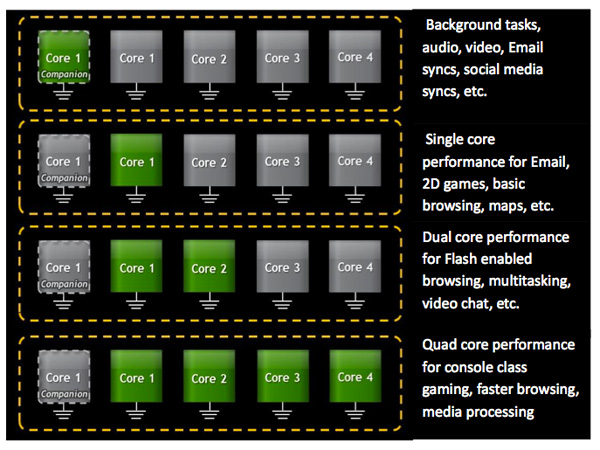
Android isn't aware of the fifth core, it only sees up to 4 at any given time. NVIDIA accomplishes this by hotplugging the cores into the scheduler. The core OS doesn't have to be modified or aware of NVIDIA's 4+1 arrangement (which it calls vSMP). NVIDIA's CPU governor code defines the specific conditions that trigger activating cores. For example, under a certain level of CPU demand the scheduler will be told there's only a single core available (the companion core). As the workload increases, the governor will sleep the companion core and enable the first GP core. If the workload continues to increase, subsequent cores will be made available to the scheduler. Similarly if the workload decreases, the cores will be removed from the scheduling pool one by one.
Courtesy NVIDIA
NVIDIA can switch between the companion and main cores in under 2ms. There's also logic to prevent wasting time flip flopping between the LP and GP cores for workloads that reside on the trigger threshold.
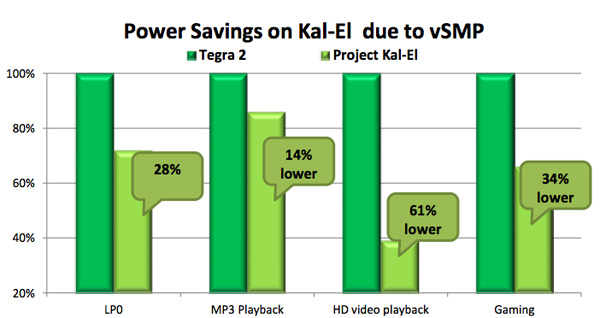
NVIDIA expects pretty much all active work to be done on the quad-core GP array, it's really only when your phone is idle and dealing with background tasks that the LP core will be in use. As a result of this process dichotomy NVIDIA is claiming significant power improvements over Tegra 2, despite an increase in transistor count:
Courtesy NVIDIA
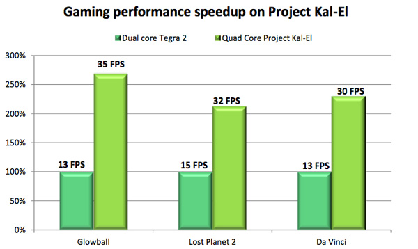
NVIDIA isn't talking about GPU performance today but it did reveal a few numbers in a new white paper:
Courtesy NVIDIA
We don't have access to the benchmarks here but everything was run on Android 3.2 at 1366 x 768 with identical game settings. The performance gains are what NVIDIA has been promising, in the 2 - 3x range. Obviously we didn't run any of these tests ourselves so approach with caution.
Final Words
What sold NVIDIA's Tegra 2 wasn't necessarily its architecture, but timing and the fact that it was Google's launch platform for Honeycomb. If the rumors are correct, NVIDIA isn't the launch partner for Ice Cream Sandwich, which means Kal-El has to stand on its own as a convincing platform.
Courtesy NVIDIA
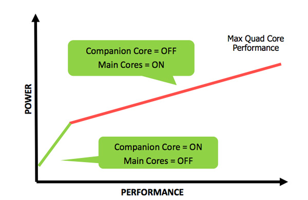
The vSMP/companion core architecture is a unique solution to the problem of increasing SoC performance while improving battery life. This is a step towards heterogenous multiprocessing, despite the homogenous implementation in Kal-El. It remains to be seen how tangible is the companion core's impact on real world battery life.


74 Comments
View All Comments
z0mb13n3d - Tuesday, September 20, 2011 - link
You're wrong, on two fronts. With Qualcomm being an architecture licensee, the Krait is not a straight-up A15 implementation (much unlike OMAP5 and Wayne, which will be). Also, if we were to assume what you're saying to be true with Qualcomm shipping retail devices based on Krait in Q1'12, realistically they would have had to have started development on their Krait architecture at least 3 years ago (especially with Qualcomm claiming that it is a new design from the ground-up). Considering this fact, the Krait will most likely be another 'in-between' architecture, straddling the A9 and A15, with custom blocks and logic in there to ensure the architecture will ramp up in frequency and be die-shrink friendly, since it has to remain competitive with current high-end A9's (Kal-El, the rumored Samsung A9 QC) and future high-end A15's (OMAP5, Wayne etc.) which are 1.5-2 years out. This is completely ignoring potential 28nm yield issues.Secondly, the whole '2x A15-class > 4x A9-class' comment is so obviously flawed, it isn't even worth the time and effort to try and put forth reasonable arguments to counter it.
metafor - Tuesday, September 20, 2011 - link
Which is why I said A15-class. Krait is not A15 but its performance -- thus released in DMIPS form -- is on the level of A15, that is to say, much more than A9."realistically they would have had to have started development on their Krait architecture at least 3 years ago (especially with Qualcomm claiming that it is a new design from the ground-up)"
Scorpion finished development in early 2009 and retailed in devices in 2010. What do you suppose the CPU team has been doing since?
"Secondly, the whole '2x A15-class > 4x A9-class' comment is so obviously flawed, it isn't even worth the time and effort to try and put forth reasonable arguments to counter it."
Oh please. Don't tell me you're one of those people who think 4x Core = 4x Performance.
z0mb13n3d - Tuesday, September 20, 2011 - link
Numbers such as DMIPS and MFLOPS do little more than help these companies position their products on paper and roadmaps. How do you know that the Krait performs on par with/beats A15's? There are no A15's around for you to compare.Scorpion finished development in early 2009? What? You clearly don't know what you're going on about here. Scorpion was available commercially in Q4 2008, implying that the 'design' was finalized much before that, most likely mid-late 2007. Assuming they started working on Krait development after that, it lends further credence to the possibility that it is a highly custom A9-based design. Given that Qualcomm has already openly stated they are planning on hitting up to 2.5GHz (!!) on Krait, it also seems very likely that it is banking on ramping up frequencies to compete with others, thereby not being a wider/higher IPC A15-based design. While it may have a leg up against Kal-El (or even Kal-El+), how it performs against pure/modified A15's (OMAP5's, future Samsung cores or Wayne) is anybody's guess.
"Oh please. Don't tell me you're one of those people who think 4x Core = 4x Performance."
...says the person who makes a silly blanket comment in the first place!
metafor - Tuesday, September 20, 2011 - link
"Numbers such as DMIPS and MFLOPS do little more than help these companies position their products on paper and roadmaps. How do you know that the Krait performs on par with/beats A15's? There are no A15's around for you to compare."ARM has provided preliminary numbers for A15 as has Qcom. Of course they are DMIPS so obviously they don't represent the bulk of workload. However, that aside, both Krait and A15 fall into a wholely different class than A9.
"Scorpion finished development in early 2009? What? You clearly don't know what you're going on about here. Scorpion was available commercially in Q4 2008"
Not really. The first revision of 8x50 was announced in 2008 but it wasn't until the second revision that you could find it in a consumer product (LG in Korea, I believe).
"Assuming they started working on Krait development after that, it lends further credence to the possibility that it is a highly custom A9-based design."
Architectural licenses don't work like that. You don't "base" it on a Cortex design. ARM doesn't give you that kind of resource (documentation, engineers, etc.). You either use a stock core or make your own. Why would a team planning on releasing a chip in 2011/2012 aim only for A9-level performance?
"Given that Qualcomm has already openly stated they are planning on hitting up to 2.5GHz (!!) on Krait, it also seems very likely that it is banking on ramping up frequencies to compete with others, thereby not being a wider/higher IPC A15-based design."
A15 is also projected to hit upwards of 2-3GHz....
Do you know anything about A15 at all? It almost doubles the pipeline length compared to A9 (8 vs 15 stages, but 8 is the load-latency whereas 15 is the number for integer exec. The load latency for A15 is ~17). It's a heavily pipelined design intended for high-frequency. It also happens to be higher in IPC as well than A9 but that came at a pretty heavy area (and likely power) cost.
z0mb13n3d - Tuesday, September 20, 2011 - link
I don't know what 'revision' you're going on about (silicon spin perhaps?...in which case you're wrong anyway), but the first QSD's were up for sampling in the Q3-Q4 08 period. The fact that the first consumer device (LG Expo) packing that particular chip shipped only a year later just goes to show why I think no Krait-based devices will ship in Q1'12Oh but you do base it off of a template! While it is up to the licensee to decide what/how much they want to customize, it'd be silly of you to think they start from 0. That kind of investment would almost never be recouped in a 3-4 year cycle. Plus, given that they did start working on Krait in late 07, performance models and simulations can give you just that, models. Part refreshes are inevitable. Look at the number of Scorpion interations!
A15 is not projected to hit anywhere CLOSE to 3GHz. The template macro limit is 2.5GHz and even that is using the G process node for the deepest pipelined model. Don't expect anything more than 1.8-2 GHz standard A15 in mobile guise.
Please stop saying stuff just for the sake of it or merely stating the obvious. Repeating the same thing again and again won't make it right!
metafor - Wednesday, September 21, 2011 - link
Yes, silicon spin. You'd be surprised how often companies claim "sampling" before silicon's remotely ready. The reason Krait SoC's should be in production by Q1 is because they were "sampling" way back in January/February of 2011.And yes, ARM licenses do work like that. You either take a stock design or you take the ISA and start from scratch. Do you have any idea how much effort it takes to reverse-engineer from RTL? You do not get detailed documentation from ARM. Have you been an ARM licensee before? Done an ARM design? Well I have. You start from 0. You can make iterative improvements as you go (although it didn't happen with Scorpion, save for MP support). But at the end of the day, trying to make major modifications to an existing ARM design without access to the original designers of that core (and you don't get that) is far more effort for too little gain.
http://www.arm.com/products/processors/cortex-a/co...
"1.5GHz-2.5 GHz quad-core configurations"
You'd be surprised what 28 HKMG can do for frequency. And yes, that is what Krait at 2.5GHz will be on.
z0mb13n3d - Wednesday, September 21, 2011 - link
If you're saying that going back to do a die re-spin after announcing commercial sampling is common in the industry, you very clearly are confused. VERY confused. This is probably the worst thing that could happen to a company. The most recent example of this would be nvidia's Fermi.Making a custom design does not imply rebuilding every single block from scratch. With proven, stable macro libraries available, it would be a criminal waste of effort, time and money to build/design every block from scratch. Likewise, to "base something" does not mean to reverse engineer code. At least not outside of Verilog assignments in school.
Finally, the link you posted proves 2 things now. One, you were clearly wrong about A15 hitting up to 3GHz. Two, that link only further proves what I've been saying all this while. To quote ARM's own implementation examples:
"Smartphone and Mobile Computing: 1 GHz – 1.5 GHz single or dual-core configurations.....
Digital Home Entertainment: 1 GHz - 2GHz..." with Home/web servers/wireless equipment estimated to hit up to 2.5GHz.
Again, please try and understand this: THESE NUMBERS ARE TEMPLATES that tell potential licensees what the architecture is capable of in terms of theoretical maximums, assuming there is no process/leakage/regulation/routing/floor planning issues. Given that a majority of existing A8/A9-based designs barely make it through more than 3/4th of a day with normal use, I can't even being to imagine what use an SoC running 4xA15's (or even 2 for that matter) at 2.5GHz would be used for. This is not even considering the power envelopes for the baseband, NAND, RAM, GPU etc.
I've said this enough number of times. It really is up to you to see things for the way they are or just go on about...random stuff. Cheers!
metafor - Thursday, September 22, 2011 - link
Lol, you say "commercial sampling" like it's some kind of magic. 8660 was "sampled" when? Oh yes, a year before commercial devices were out. 8x50 was "sampled" when? Oh yes, a year before devices were out. Tegra 2 was "sampled" when? Oh man. Let's go to Kal-el."Making a custom design does not imply rebuilding every single block from scratch. With proven, stable macro libraries available, it would be a criminal waste of effort, time and money to build/design every block from scratch."
It does mean building every single block. Including the circuit macros for the standard cells. Sure, you could use ARM's standard cell library, but they were made specifically for the micro-architecture of the ARM cores. You may need your wallace tree to have faster compressors, your register files to have better access times or more ports or lower standby power. And you get no documentation for any of the individual modules. You get a behavior model of the whole CPU and verilog; that's it. Think about how much effort it takes to go in to a submodule and figure out "hey, what are the small details here that I don't know".
Again, have you actually done an ARM design? You sound awfully sure of yourself.
As for the rest of your ranting, all I've said is that A15 is targeting the same frequency at 28HKMG as Krait. Which is, as I've shown, true.
Lucian Armasu - Wednesday, September 21, 2011 - link
A Cortex A15 is significantly larger than a Cortex A9, so by itself should be a power hog compared to A9, but the 28nm process should eliminate part of that, plus whatever optimizations Nvidia and the others do to it by then. Plus, there isn't any quad core Cortex A15 chip coming to market, perhaps besides Wayne/Tegra4, which will *probably* have that.TI OMAP 5 is not a quad core Cortex A15. It only has 2 Cortex A15 cores at 2.5 Ghz each, and it's coming late 2012. The other MP4 cores are companion cores, but I believe work differently than Nvidia's companion core. We'll probably see a quad core Krait chip from Qualcomm in 2nd half of 2012 at 2.5 Ghz, but I imagine each of that core should be a bit weaker than a Cortex A15 core.
dagamer34 - Tuesday, September 20, 2011 - link
Ehh??? You missed the most important info on the first slide: Windows Phone is on there! To date, only Qualcomm chips have been used in Windows Phone devices.