Intel's Ivy Bridge Architecture Exposed
by Anand Lal Shimpi on September 17, 2011 2:00 AM EST- Posted in
- CPUs
- Intel
- Ivy Bridge
- IDF 2011
- Trade Shows
Core Architecture Changes
Ivy Bridge is considered a tick from the CPU perspective but a tock from the GPU perspective. On the CPU core side that means you can expect clock-for-clock performance improvements in the 4 - 6% range. Despite the limited improvement in core-level performance there's a lot of cleanup that went into the design. In order to maintain a strict design schedule it's not uncommon for a number of features not to make it into a design, only to be added later in the subsequent product. Ticks are great for this.


Five years ago Intel introduced Conroe which defined the high level architecture for every generation since. Sandy Bridge was the first significant overhaul since Conroe and even it didn't look very different from the original Core 2. Ivy Bridge continues the trend.
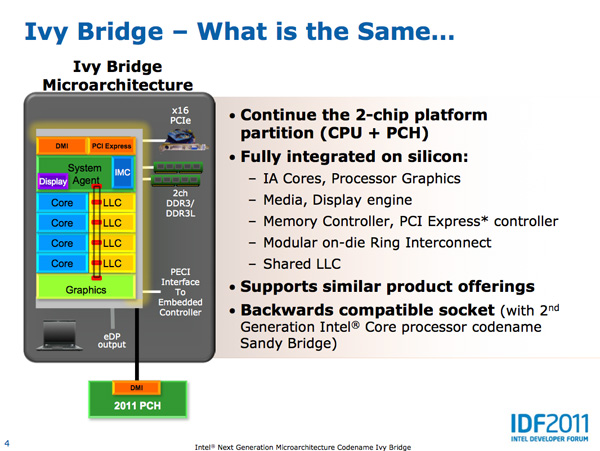
The front end in Ivy Bridge is still 4-wide with support for fusion of both x86 instructions and decoded uOps. The uOp cache introduced in Sandy Bridge remains in Ivy with no major changes.
Some structures within the chip are now better optimized for single threaded execution. Hyper Threading requires a bunch of partitioning of internal structures (e.g. buffers/queues) to allow instructions from multiple threads to use those structures simultaneously. In Sandy Bridge, many of those structures are statically partitioned. If you have a buffer that can hold 20 entries, each thread gets up to 10 entries in the buffer. In the event of a single threaded workload, half of the buffer goes unused. Ivy Bridge reworks a number of these data structures to dynamically allocate resources to threads. Now if there's only a single thread active, these structures will dedicate all resources to servicing that thread. One such example is the DSB queue that serves the uOp cache mentioned above. There's a lookup mechanism for putting uOps into the cache. Those requests are placed into the DSB queue, which used to be split evenly between threads. In Ivy Bridge the DSB queue is allocated dynamically to one or both threads.
In Sandy Bridge Intel did a ground up redesign of its branch predictor. Once again it doesn't make sense to redo it for Ivy Bridge so branch prediction remains the same. In the past prefetchers have stopped at page boundaries since they are physically based. Ivy Bridge lifts this restriction.
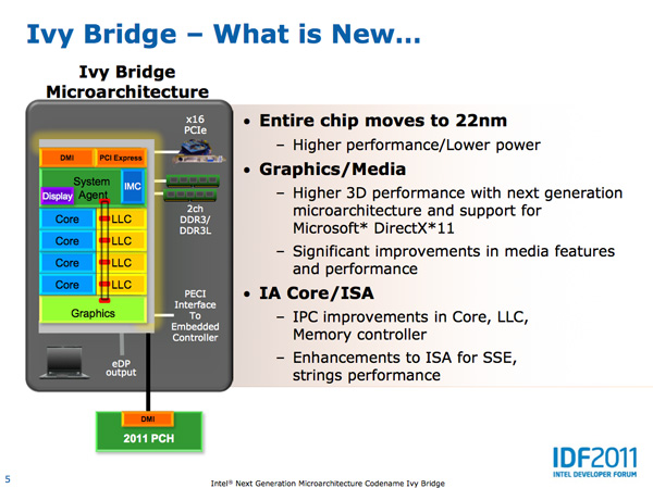
The number of execution units hasn't changed in Ivy Bridge, but there are some changes here. The FP/integer divider sees another performance gain this round. Ivy Bridge's divider has twice the throughput of the unit in Sandy Bridge. The advantage here shows up mostly in FP workloads as they tend to be more computationally heavy.
MOV operations can now take place in the register renaming stage instead of making it occupy an execution port. The x86 MOV instruction simply copies the contents of a register into another register. In Ivy Bridge MOVs are executed by simply pointing one register at the location of the destination register. This is enabled by the physical register file first introduced in Sandy Bridge, in addition to a whole lot of clever logic within IVB. Although MOVs still occupy decode bandwidth, the instruction doesn't take up an execution port allowing other instructions to execute in place of it.
ISA Changes
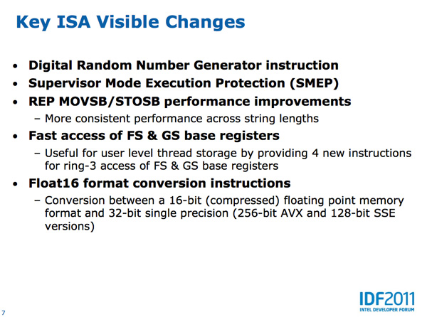
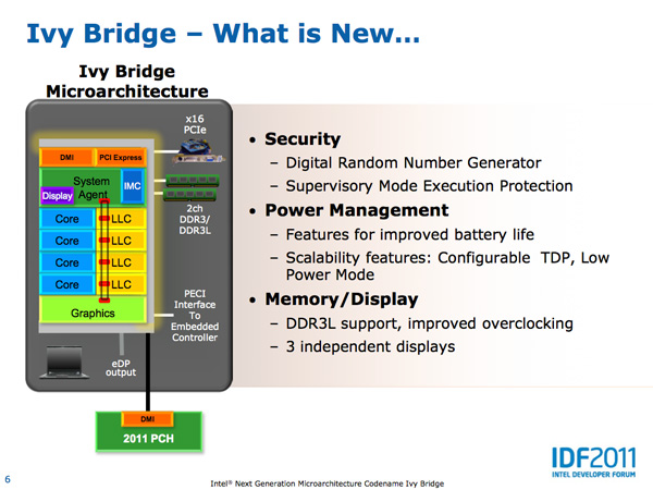
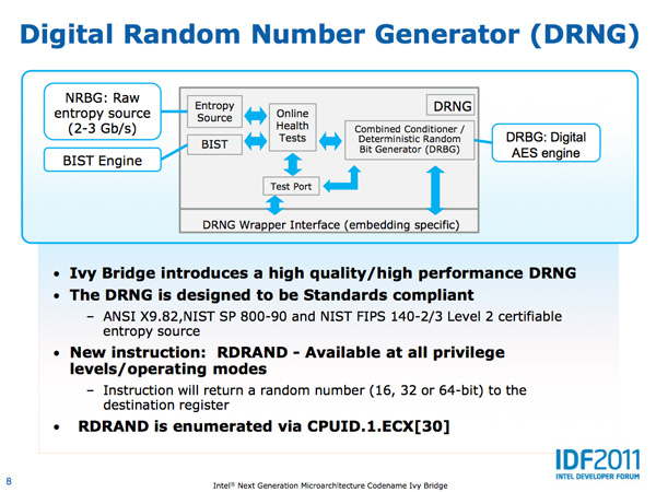
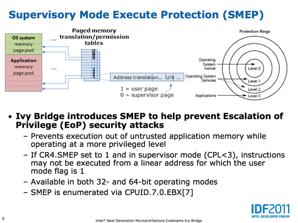
Intel also introduced a number of ISA changes in Ivy Bridge. The ones that stand out the most to me are the inclusion of a very high speed digital random number generator (DRNG) and supervisory mode execution protection (SMEP).
Ivy Bridge's DRNG can generate high quality random numbers (standards compliant) at 2 - 3Gbps. The DRNG is available to both user and OS level code. This will be very important for security and algorithms going forward.
SMEP in Ivy Bridge provides hardware protection against user mode code being executed in more privileged levels.


97 Comments
View All Comments
driscoll42 - Saturday, September 17, 2011 - link
On the last page there's "Should the fab engineers at Intel do their job well, Ivy Bridge could deliver much better power characteristics than Ivy." in the second paragraph, should that be Sandy on the end?Anand Lal Shimpi - Saturday, September 17, 2011 - link
Thank you! Fixed :)Take care,
Anand
Beenthere - Saturday, September 17, 2011 - link
It's good that Intel has decided that their GPU sucks and that to be competitive they need to catch up to AMD. This will take some time as AMD has a two year head start on APUs but it's all good for consumers.In spite of the marketing hype from Intel it looks like they've conceded that AMD has the better system approach with APUs for mainstream consumers and laptops. CPU performance alone is no longer a valid yardstick for PC performance thanks to AMD's advance thinking and Llano.
TypeS - Saturday, September 17, 2011 - link
I realize Intel is behind (has been for since anyone can remember) in the graphics arena compared to AMD/ATI and NVIDIA, but is AMD "two years ahead" in terms of an APU? While Clarkdale can't really be considered a true all in one package (hey remember when Kentsfield wasn't considered a true quad core?), it was still an all in one package, and with Sandy Bridge, Intel brought it all together onto one die. Intel isn't calling it an APU but if you compare SNB and Llano/Bulldozer, they share some similarities.AMD's edge is on graphics, and Intel is closing the gap.
I might be missing something though in why you say they are ahead in terms of an "APU", but from my knowledge, Intel as first to release a retail/commercial APU.
Guspaz - Monday, September 19, 2011 - link
Intel might be catching up in terms of physical performance, but Intel's drivers still, quite frankly, suck. It's the one thing really holding the platform back, in terms of both compatibility and performance. Even simple things like flash acceleration can sometimes be wonky with Intel's drivers.Furthermore, developers like Carmack have been pestering Intel to give them lower-level access to the hardware, with potentially enormous performance benefits; they'd like to treat PCs more like a console, and stripping away much of the driver/graphics overhead (particularly in terms of memory management) could see some pretty big performance gains. There's a reason why modern integrated GPUs like in Ivy Bridge have theoretical performance on-par with a 360 or PS3, but in practice, are nowhere near as performant.
Of course, the same is true for AMD and nVidia; high-end developers like Carmack and Sweeney seem to want lower-level access to hardware. From Carmack's latest QuakeCon keynote, it does seem like the hardware manufacturers are listening.
fic2 - Monday, September 19, 2011 - link
Yeah, Intel seems to want to catch up and made a pretty decent effort of no sucking with the HD3000. BUT then they go and do a dumb@ss thing like put the crappy HD2000 on 90% of the Sandies they sell. I think if marketing would get the he11 out of the way they wouldn't be too sucky.Oh, yeah, except the drivers.
bigboxes - Saturday, September 17, 2011 - link
I love AMD as much as the next guy (have three running AMD boxes), but are you going to continue to be "that guy" that posts this nonsense in every Intel/AMD thread? We get it. You love AMD and want to help them win the CPU wars. Yay for fanbois everywhere!Beenthere - Saturday, September 17, 2011 - link
Intel hasn't released an APU. They have released a CPU and GPU on the same slab of silicon. That's not an integrated APU.No nonsense, just facts. I like facts. Some folks can't handle facts but that's life. I like choice and scrupulous businesses. That's what AMD is unlike Intel.
ltcommanderdata - Saturday, September 17, 2011 - link
For someone arguing against marketing hype and looking for facts you seem overly preoccupied by AMD's APU term. If you are looking for which product currently on the market has tighter CPU/IGP integration then that produce is Sandy Bridge not Llano. For instance Sandy Bridge allows bidirectional communication/sharing of instructions and data between the CPUs and IGP via a shared on die L3 cache instead of through a crossbar and off die system memory as in Llano. Sandy Bridge also has more advanced power and thermal monitoring allowing efficient sharing of TDP room between the CPU and IGP, allowing each to be overclocked as needed, something Llano doesn't do.Yes, Llano has the faster GPU, but that's not the critical concern if what you are interested in is integration. Intel's CPU and GPU on a slab of silicon was Arrandale. Sandy Bridge has moved well beyond that. Llano's CPU/GPU integration looks to be somewhere in between Arrandale and Sandy Bridge. Seeing Llano is AMD's 1st generation Fusion product along with Brazos that's fine. But just because AMD's calls their product an APU doesn't mean it's the pinnacle of CPU/GPU integration.
gramboh - Sunday, September 18, 2011 - link
Boom. Beenthere just got roasted, and of course disappears rather than admitting he was wrong.