NVIDIA's GeForce GTX 580: Fermi Refined
by Ryan Smith on November 9, 2010 9:00 AM ESTMeet the GTX 580
Since we’ve already discussed the cooling, let’s dive right in to the rest of the GTX 580, shall we?
Launching today will be a single GTX 580 design, the reference design. Talking to our contacts, semi-custom designs (designs using the reference PCB with a different cooler) are due in the next few weeks assuming everything goes to plan and of course there’s ample supply. And while we’re on that note, NVIDIA let us know that with their focus on cooling on the GTX 580 they aren’t going to be letting custom GTX 580 designs go out without a more thorough inspection. The acoustic performance of the reference GTX 580 is going to be the bare minimum to get a design approved – if it can’t beat the reference design, NVIDIA won’t allow it. We consider this a matter of brand protection for the company, as a bad/loud GeForce is still a GeForce all the same.
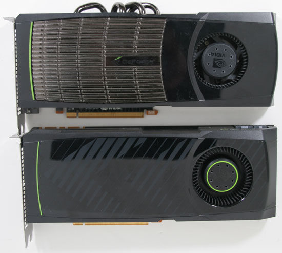
Top: GTX 480. Bottom: GTX580
With the reference design the resulting card is very close to being a GTX 285/480 hybrid. In terms of overall design it ends up looking very similar to the GTX 285. At 10.5” long it’s the same length as the GTX 480 or a smidge longer than the GTX 285, and should fit in to any cases those cards could work in. Power connectivity is the same as the GTX 480, with 6pin and 8pin PCIe sockets being located at the top of the card, providing easy access to the sockets. At 244W TDP the card draws too much for 6+6, but you can count on an eventual GTX 570 to fill that niche. Meanwhile NVIDIA has kept the 480’s detachable shroud lid, meaning you can remove the cover of the shroud without disturbing the rest of the card; it’s worth noting that it’s secured with screws rather than laches this time however.
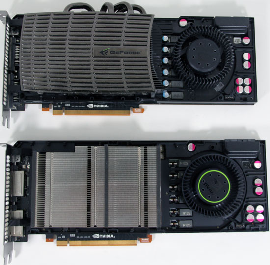
Heatsinks Exposed! Top: GTX 480. Bottom: GTX 580
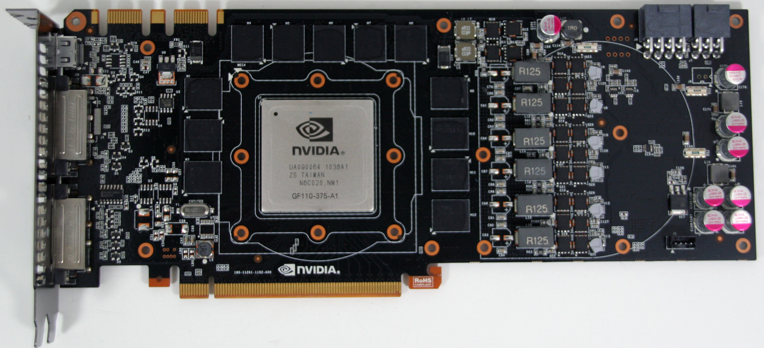
On the front side of the PCB you’ll find the 12 GDDR5 chips composing the card’s 384bit memory bus. The thermal pads connecting the memory to the shroud have once again wiped out the chip markings, so we haven’t been able to determine what these chips are, although we’re confident they’re 5Gbps like in past cards. At the center of the card is the GF110 GPU encased in a metal heatspreader, a common sight for NVIDIA’s high-end GPUs. This is an A1 revision GPU, which in NVIDIA’s counting system means it’s the first tape-out. Elsewhere on the board you’ll find the 2 SLI connectors, providing support for tri-SLI on the 580. All told while the GPU has been refined, the PCB remains largely unchanged from the GTX 480 other than removing the ventilation holes – all of the ICs are in practically the same place, and even the VRM controller is the same.
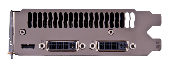
Meanwhile looking at the IO bracket for the 580, we find the same configuration as we saw on the 480. Below a full-sized vent are 2 DVI ports and a mini-HDMI port. NVIDIA slightly revised their display controller for GF110/GTX580; the good news is that HDMI 1.4a is supported, the bad news is that full audio bitstreaming is not supported so it’s the same as it was on the GTX 480: 8 channel LPCM and lossy audio formats like DD+ and DTS. This actually caught us off-guard since we were expecting the full GF104 treatment here, but it just goes to show that this is a GF100-derrivative after all. Unfortunately this also extends to the number of displays supported – NVIDIA still only supports 2 displays on one card, so you need to run in SLI if you intend to take advantage of 3DVision/NVIDIA surround across 3 monitors.
Finally, it’s with some sense of irony that we find ourselves yelling more at AMD than NVIDIA for naming shenanigans this time around, considering it was NVIDIA that brought us the 8800GT/9800GT and GeForce 200/300 product naming snafus. While NVIDIA has made some changes compared to the GTX 480, it’s a very short list; shorter than even AMD’s list for the 6800 series. At the same time, at least the GTX 580 is faster than the GTX 480 versus AMD’s 6800/5800 series. Quite frankly the GTX 580 should be the GTX 485 – the few architectural changes we’ve seen do make a difference, but then NVIDIA did a whole die shrink on the GTX 280 and only got a GTX 285 out of it. Both companies seem committed to coming out with a new family of video cards this year regardless of where the GPU powering them has actually changed. Ultimately the GTX 580 is the second flimsiest excuse for a new series number, next only to simply rebranding an existing GPU.


160 Comments
View All Comments
cjb110 - Tuesday, November 9, 2010 - link
"The thermal pads connecting the memory to the shroud have once again wiped out the chip markets", wow powerful adhesive that! Bet Intel's pissed.cjb110 - Tuesday, November 9, 2010 - link
"While the difference is’ earthshattering, it’s big enough..." nt got dropped, though not yet at my workplace:)Invader Mig - Tuesday, November 9, 2010 - link
I don't know the stance on posting links to other reviews since I'm a new poster, so I wont. I would like to make note that in another review they claim to have found a work around the power throttling that allowed them to use furmark to get accurate temps and power readings. This review has the 580 at 28w above the 480 at max load. I don't mean to step on anyone's toe's, but I have seen so many different numbers because of this garbage nvidia has pulled, and the only person who claims to have furmark working gets higher numbers. I would really like to see something definitive.7Enigma - Tuesday, November 9, 2010 - link
Here's my conundrum. What is the point of something like Furmark that has no purpose except to overstress a product? In this case the 580 (with modified X program) doesn't explode and remains within some set thermal envelope that is safe to the card. I like using Crysis as it's a real-world application that stresses the GPU heavily.Until we have another game/program that is used routinely (be it game or coding) that surpasses the heat generation and power draw of Crysis I just don't see the need to try to max out the cards with a benchmark. OC your card to the ends of the earth and run something real, that is understandable. But just using a program that has no real use to artificially create a power draw just doesn't have any benefit IMO.
Gonemad - Tuesday, November 9, 2010 - link
I beg to differ. (be careful, high doses of flaming.)Let me put it like this. The Abrams M1 Tank is tested on a 60º ramp (yes, that is sixty degrees), where it must park. Just park there, hold the brakes, and then let go. It proves the brakes on a 120-ton 1200hp vehicle will work. It is also tested on emergency brakes, where this sucker can pull a full stop from 50mph on 3 rubber-burning meters. (The treads have rubber pads, for the ill informed).
Will ever a tank need to hold on a 60º ramp? Probably not. Would it ever need to come to a screeching halt in 3 meters? In Iraqi, they probably did, in order to avoid IEDs. But you know, if there were no prior testing, nobody would know.
I think there should be programs specifically designed to stress the GPU in unintended ways, and it must protect itself from destruction, regardless of what code is being thrown at it. NVIDIA should be grateful somebody pointed that out to them. AMD was thankful when they found out the 5800 series GPUs (and others, but this was worse) had lousy performance on 2D acceleration, or none at all, and rushed to fix its drivers. Instead, NVIDIA tries to cheat Furmark by recognizing its code and throttling. Pathetic.
Perhaps someday, a scientific application may come up with repeatable math operations that just behave exactly like Furmark. So, out of the blue, you got a $500 worth of equipment that gets burned out, and nobody can tell why??? Would you like that happening to you? Wouldn't you like to be informed that this or that code, at least, could destroy your equipment?
What if Furmark wasn't designed to stress GPUs, but it was an actual game, (with furry creatures, lol)?
Ever heard of Final Fantasy XIII killing off PS3s for good, due to overload, thermal runaway, followed by meltdown? Rumors are there, if you believe them is entirely to you.
Ever heard of Nissan GTR (skyline) being released with a top-speed limiter with GPS that unlocks itself when the car enters the premises of Nissan-approved racetracks? Inherent safety, or meddling? Can't you drive on a Autoban at 300km/h?
Remember back in the day of early benchmark tools, (3DMark 2001 if I am not mistaken), where the Geforce drivers detected the 3DMark executable and cheated the hell out of the results, and some reviewers got NVIDIA red-handed when they renamed and changed the checksum of the benchmark??? Rumors, rumors...
The point is, if there is a flaw, a risk of an unintended instruction kill the hardware, the buyer should be rightfully informed of such conditions, specially if the company has no intention at all to fix it. Since Anand warned us, they will probably release the GTX 585 with full hardware thermal safeties. Or new drivers. Or not.
Just like the instruction #PROCHOT was inserted in the Pentium (which version?) and some reviewers tested it against an AMD chip. I never forgot that AMD processor billowing blue smoke the moment the heatsink was torn off. Good PR, bad PR. The video didn´t look fake to me back then, just unfair.
In the end, it becomes matter of PR. If suddenly all the people that played Crysis on this card caused it to be torched, we would have something really interesting.
Sihastru - Tuesday, November 9, 2010 - link
AMD has a similar system in place since the HD4xx0 generation. Remember when Furmark used to blow up 48x0 cards? Of course not. But look it up...What nVidia did here is what AMD has in all their mid/high end cards since HD4xx0. At least nVidia will only throttle when it detects Furmark/OCCT. AMD cards will throttle in any situation if the power limiter requires it.
JimmiG - Tuesday, November 9, 2010 - link
It's a very unfortunate situation that both companies are to blame for. That's what happens when you push the limits of power consumption and heat output too far while at the same time trying to keep manufacturing costs down.The point of a stress test is to push the system to the very limit (but *not* beyond it, like AMD and Nvidia would have you believe). You can then be 100% assured that it will run all current and future games and HPC applications, not matter what unusual workloads they dump on your GPU or CPU, without crashes or reduced performance.
cactusdog - Tuesday, November 9, 2010 - link
So if you want to use multiple monitors do you still need 2 cards to run it or have they enabled a third monitor on the 580?Sihastru - Tuesday, November 9, 2010 - link
Yes.Haydyn323 - Tuesday, November 9, 2010 - link
The 580 as with the previous generation still only supports 2 monitors max per card.