NVIDIA's GeForce GTX 580: Fermi Refined
by Ryan Smith on November 9, 2010 9:00 AM ESTMeet the GTX 580
Since we’ve already discussed the cooling, let’s dive right in to the rest of the GTX 580, shall we?
Launching today will be a single GTX 580 design, the reference design. Talking to our contacts, semi-custom designs (designs using the reference PCB with a different cooler) are due in the next few weeks assuming everything goes to plan and of course there’s ample supply. And while we’re on that note, NVIDIA let us know that with their focus on cooling on the GTX 580 they aren’t going to be letting custom GTX 580 designs go out without a more thorough inspection. The acoustic performance of the reference GTX 580 is going to be the bare minimum to get a design approved – if it can’t beat the reference design, NVIDIA won’t allow it. We consider this a matter of brand protection for the company, as a bad/loud GeForce is still a GeForce all the same.
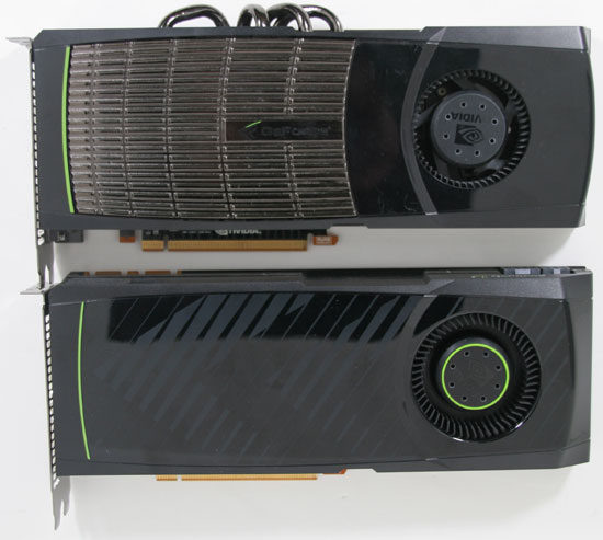
Top: GTX 480. Bottom: GTX580
With the reference design the resulting card is very close to being a GTX 285/480 hybrid. In terms of overall design it ends up looking very similar to the GTX 285. At 10.5” long it’s the same length as the GTX 480 or a smidge longer than the GTX 285, and should fit in to any cases those cards could work in. Power connectivity is the same as the GTX 480, with 6pin and 8pin PCIe sockets being located at the top of the card, providing easy access to the sockets. At 244W TDP the card draws too much for 6+6, but you can count on an eventual GTX 570 to fill that niche. Meanwhile NVIDIA has kept the 480’s detachable shroud lid, meaning you can remove the cover of the shroud without disturbing the rest of the card; it’s worth noting that it’s secured with screws rather than laches this time however.
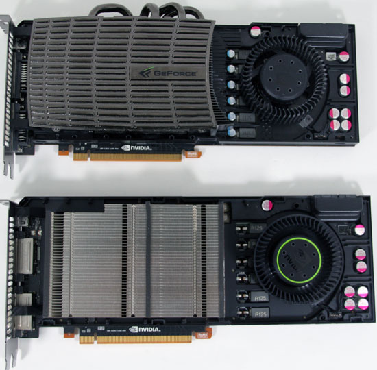
Heatsinks Exposed! Top: GTX 480. Bottom: GTX 580
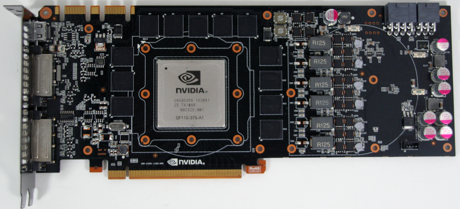
On the front side of the PCB you’ll find the 12 GDDR5 chips composing the card’s 384bit memory bus. The thermal pads connecting the memory to the shroud have once again wiped out the chip markings, so we haven’t been able to determine what these chips are, although we’re confident they’re 5Gbps like in past cards. At the center of the card is the GF110 GPU encased in a metal heatspreader, a common sight for NVIDIA’s high-end GPUs. This is an A1 revision GPU, which in NVIDIA’s counting system means it’s the first tape-out. Elsewhere on the board you’ll find the 2 SLI connectors, providing support for tri-SLI on the 580. All told while the GPU has been refined, the PCB remains largely unchanged from the GTX 480 other than removing the ventilation holes – all of the ICs are in practically the same place, and even the VRM controller is the same.
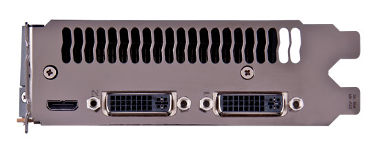
Meanwhile looking at the IO bracket for the 580, we find the same configuration as we saw on the 480. Below a full-sized vent are 2 DVI ports and a mini-HDMI port. NVIDIA slightly revised their display controller for GF110/GTX580; the good news is that HDMI 1.4a is supported, the bad news is that full audio bitstreaming is not supported so it’s the same as it was on the GTX 480: 8 channel LPCM and lossy audio formats like DD+ and DTS. This actually caught us off-guard since we were expecting the full GF104 treatment here, but it just goes to show that this is a GF100-derrivative after all. Unfortunately this also extends to the number of displays supported – NVIDIA still only supports 2 displays on one card, so you need to run in SLI if you intend to take advantage of 3DVision/NVIDIA surround across 3 monitors.
Finally, it’s with some sense of irony that we find ourselves yelling more at AMD than NVIDIA for naming shenanigans this time around, considering it was NVIDIA that brought us the 8800GT/9800GT and GeForce 200/300 product naming snafus. While NVIDIA has made some changes compared to the GTX 480, it’s a very short list; shorter than even AMD’s list for the 6800 series. At the same time, at least the GTX 580 is faster than the GTX 480 versus AMD’s 6800/5800 series. Quite frankly the GTX 580 should be the GTX 485 – the few architectural changes we’ve seen do make a difference, but then NVIDIA did a whole die shrink on the GTX 280 and only got a GTX 285 out of it. Both companies seem committed to coming out with a new family of video cards this year regardless of where the GPU powering them has actually changed. Ultimately the GTX 580 is the second flimsiest excuse for a new series number, next only to simply rebranding an existing GPU.


160 Comments
View All Comments
chizow - Tuesday, November 9, 2010 - link
There's 2 ways they can go with the GTX 570, either more disabled SM than just 1 (2-3) and similar clockspeed to the GTX 580, or fewer disabled SM but much lower clockspeed. Both would help to reduce TDP but with more disabled SM that would also help Nvidia unload the rest of their chip yield. I have a feeling they'll disable 2-3 SM with higher clocks similar to the 580 so that the 470 is still slightly slower than the 480.I'm thinking along the same lines as you though for the GTX 560, it'll most likely be the full-fledged GF104 we've been waiting for with all 384SP enabled, probably slightly higher clockspeeds and not much more than that, but definitely a faster card than the original GF104.
vectorm12 - Tuesday, November 9, 2010 - link
I'd really love to see the raw crunching power of the 480/580 vs. 5870/6870.I've found ighashgpu to be a great too to determine that and it can be found at http://www.golubev.com/
Please consider it for future tests as it's very well optimized for both CUDA and Stream
spigzone - Tuesday, November 9, 2010 - link
The performance advantage of a single GPU vs CF or SLI is steadily diminishing and approaching a point of near irrelevancy.6870 CF beats out the 580 in nearly every parameter, often substantially on performance benchmarks, and per current newegg prices, comes in at $80 cheaper.
But I think the real sweet spot would be a 6850 CF setup with AMD Overdrive applied 850Mz clocks, which any 6850 can achieve at stock voltages with minimal thermal/power/noise costs (and minimal 'tinkering'), and from the few 6850 CF benchmarks that showed up would match or even beat the GTX580 on most game benchmarks and come in at $200 CHEAPER.
That's an elbow from the sky in my book.
smookyolo - Tuesday, November 9, 2010 - link
You seem to be forgetting the minimum framerates... those are so much more important than average/maximum.Sihastru - Tuesday, November 9, 2010 - link
Agreed, CF scales very badly when it comes to minumum framerates. It is even below the minimum framerates of one of the cards in the CF setup. It is very anoying when you're doing 120FPS in a game and from time to time your framerates drop to an unplayable and very noticable 20FPS.chizow - Tuesday, November 9, 2010 - link
Nice job on the review as usual Ryan,Would've liked to have seen some expanded results however, but somewhat understandable given your limited access to hardware atm. It sounds like you plan on having some SLI results soon.
I would've really liked to have seen clock-for-clock comparisons though to the original GTX 480 though to isolate the impact of the refinements between GF100 and GF110. To be honest, taking away the ~10% difference in clockspeeds, what we're left with seems to be ~6-10% from those missing 6% functional units (32 SM and 4 TMUs).
I would've also liked to have seen some preliminary overclocking results with the GF110 to see how much the chip revision and cooling refinements increased clockspeed overhead, if at all. Contrary to somewhat popular belief, the GTX 480 did overclock quite well, and while that also increased heat and noise it'll be hard for someone with an overclocked 480 to trade it in for a 580 if it doesn't clock much better than the 480.
I know you typically have follow-up articles once the board partners send you more samples, so hopefully you consider these aspects in your next review, thanks!
PS: On page 4, I believe this should be a supposed GTX 570 mentioned in this excerpt and not GTX 470: "At 244W TDP the card draws too much for 6+6, but you can count on an eventual GTX 470 to fill that niche."
mapesdhs - Tuesday, November 9, 2010 - link
"I would've also liked to have seen some preliminary overclocking results ..."
Though obviously not a true oc'ing revelation, I note with interest there's already
a factory oc'd 580 listed on seller sites (Palit Sonic), with an 835 core and 1670
shader. The pricing is peculiar though, with one site pricing it the same as most
reference cards, another site pricing it 30 UKP higher. Of course though, none
of them show it as being in stock yet. :D
Anyway, thanks for the writeup! At least the competition for the consumer finally
looks to be entering a more sensible phase, though it's a shame the naming
schemes are probably going to fool some buyers.
Ian.
Ryan Smith - Wednesday, November 10, 2010 - link
You're going to have to wait until I have some more cards for some meaningful overclocking results. However clock-for-clock comparisons I can do.http://www.anandtech.com/show/4012/nvidias-geforce...
JimmiG - Tuesday, November 9, 2010 - link
Well technically, this is not a 512-SP card at 772 MHz. This is because if you ever find a way to put all 512 processors at 100% load, the throttling mechanism will kick in.That's like saying you managed to overclock your CPU to 4.7 GHz.. sure, it might POST, but as soon as you try to *do* anything, it instantly crashes.
Ryan Smith - Tuesday, November 9, 2010 - link
Based on the performance of a number of games and compute applications, I am confident that power throttling is not kicking in for anything besides FurMark and OCCT.