NVIDIA's GeForce GTX 580: Fermi Refined
by Ryan Smith on November 9, 2010 9:00 AM ESTMeet the GTX 580
Since we’ve already discussed the cooling, let’s dive right in to the rest of the GTX 580, shall we?
Launching today will be a single GTX 580 design, the reference design. Talking to our contacts, semi-custom designs (designs using the reference PCB with a different cooler) are due in the next few weeks assuming everything goes to plan and of course there’s ample supply. And while we’re on that note, NVIDIA let us know that with their focus on cooling on the GTX 580 they aren’t going to be letting custom GTX 580 designs go out without a more thorough inspection. The acoustic performance of the reference GTX 580 is going to be the bare minimum to get a design approved – if it can’t beat the reference design, NVIDIA won’t allow it. We consider this a matter of brand protection for the company, as a bad/loud GeForce is still a GeForce all the same.
Top: GTX 480. Bottom: GTX580
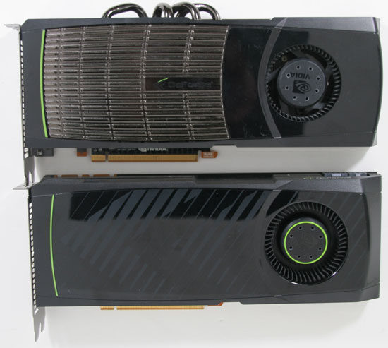
With the reference design the resulting card is very close to being a GTX 285/480 hybrid. In terms of overall design it ends up looking very similar to the GTX 285. At 10.5” long it’s the same length as the GTX 480 or a smidge longer than the GTX 285, and should fit in to any cases those cards could work in. Power connectivity is the same as the GTX 480, with 6pin and 8pin PCIe sockets being located at the top of the card, providing easy access to the sockets. At 244W TDP the card draws too much for 6+6, but you can count on an eventual GTX 570 to fill that niche. Meanwhile NVIDIA has kept the 480’s detachable shroud lid, meaning you can remove the cover of the shroud without disturbing the rest of the card; it’s worth noting that it’s secured with screws rather than laches this time however.
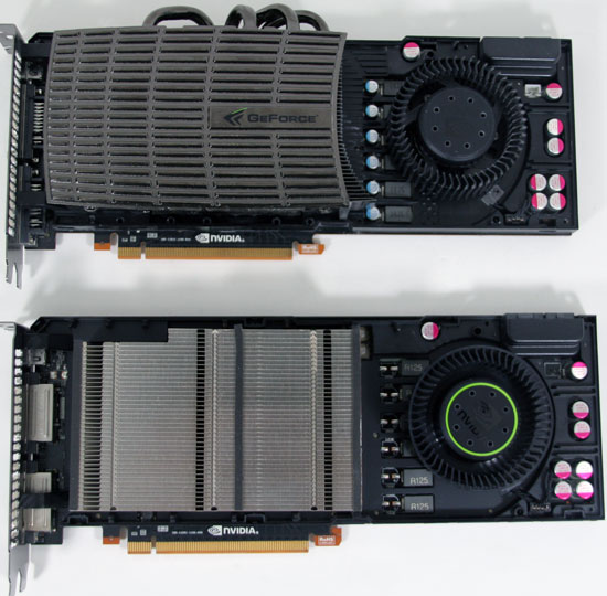
Heatsinks Exposed! Top: GTX 480. Bottom: GTX 580
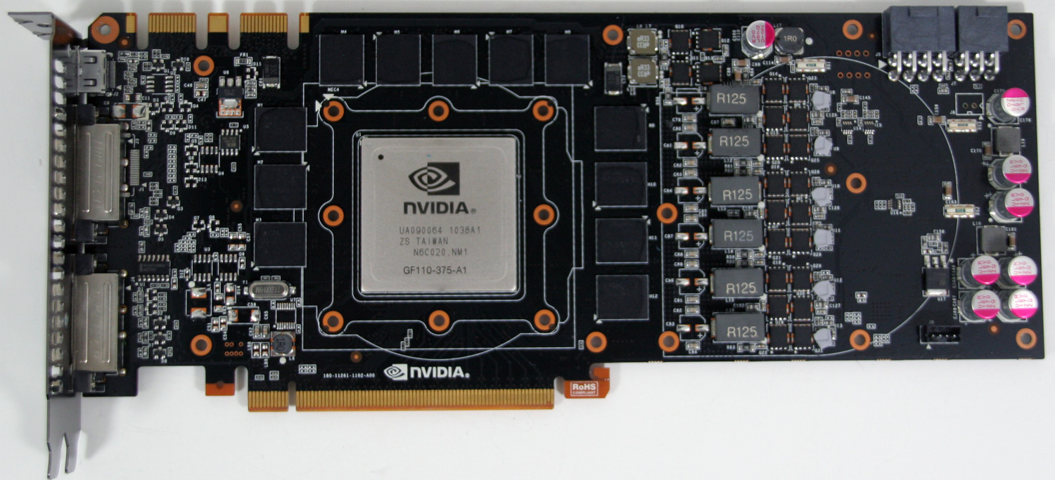
On the front side of the PCB you’ll find the 12 GDDR5 chips composing the card’s 384bit memory bus. The thermal pads connecting the memory to the shroud have once again wiped out the chip markings, so we haven’t been able to determine what these chips are, although we’re confident they’re 5Gbps like in past cards. At the center of the card is the GF110 GPU encased in a metal heatspreader, a common sight for NVIDIA’s high-end GPUs. This is an A1 revision GPU, which in NVIDIA’s counting system means it’s the first tape-out. Elsewhere on the board you’ll find the 2 SLI connectors, providing support for tri-SLI on the 580. All told while the GPU has been refined, the PCB remains largely unchanged from the GTX 480 other than removing the ventilation holes – all of the ICs are in practically the same place, and even the VRM controller is the same.
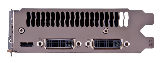
Meanwhile looking at the IO bracket for the 580, we find the same configuration as we saw on the 480. Below a full-sized vent are 2 DVI ports and a mini-HDMI port. NVIDIA slightly revised their display controller for GF110/GTX580; the good news is that HDMI 1.4a is supported, the bad news is that full audio bitstreaming is not supported so it’s the same as it was on the GTX 480: 8 channel LPCM and lossy audio formats like DD+ and DTS. This actually caught us off-guard since we were expecting the full GF104 treatment here, but it just goes to show that this is a GF100-derrivative after all. Unfortunately this also extends to the number of displays supported – NVIDIA still only supports 2 displays on one card, so you need to run in SLI if you intend to take advantage of 3DVision/NVIDIA surround across 3 monitors.
Finally, it’s with some sense of irony that we find ourselves yelling more at AMD than NVIDIA for naming shenanigans this time around, considering it was NVIDIA that brought us the 8800GT/9800GT and GeForce 200/300 product naming snafus. While NVIDIA has made some changes compared to the GTX 480, it’s a very short list; shorter than even AMD’s list for the 6800 series. At the same time, at least the GTX 580 is faster than the GTX 480 versus AMD’s 6800/5800 series. Quite frankly the GTX 580 should be the GTX 485 – the few architectural changes we’ve seen do make a difference, but then NVIDIA did a whole die shrink on the GTX 280 and only got a GTX 285 out of it. Both companies seem committed to coming out with a new family of video cards this year regardless of where the GPU powering them has actually changed. Ultimately the GTX 580 is the second flimsiest excuse for a new series number, next only to simply rebranding an existing GPU.


160 Comments
View All Comments
knutjb - Tuesday, November 9, 2010 - link
I agree guys it should be a 485 not a 580.The 6870 is a sore spot on an otherwise solid refinement. Curious to see its SLI performance. $559 on Newegg this am.
dtham - Tuesday, November 9, 2010 - link
Anyone know if aftermarket cooling for the GTX 480 will work for the GTX 580? It would be great to be able to reuse a waterblock from a GTX 480 for the new 580s. Looking at the picture the layout looks similar.mac2j - Tuesday, November 9, 2010 - link
In Europe the GTX 580 was launched at 399 Euros and in response ATI has lowered the 5970 to 389 Euros (if you believe the rumors).This can only bode well for holiday prices of the 6970 vs 580.
samspqr - Tuesday, November 9, 2010 - link
it's already listed and in stock at alternate.de, but the cheapest one is 480eurthe only 5970 still in stock there is 540eur
yzkbug - Tuesday, November 9, 2010 - link
I moved all my gaming to the living room on a big screen TV and HTPC (a next next gen console in a sense). But, Optimus would be the only way to use this card on HTPC.slatr - Tuesday, November 9, 2010 - link
Ryan,Would you be able to test with Octane Renderer?
I am interested to see if Octane gets throttled.
Thanks
Andyburgos - Tuesday, November 9, 2010 - link
Ryan:I hold you in the most absolute respect. Actually, in my first post a while ago I praised your work, and I think you´re quite didactic and fun to read. On that, thanks for the review.
However, I need to ask you: W.T.F. is wrong with you? Aren´t you pissed off by the fact that GTX480 was a half baked chip (wouldn´t say the same about GTX460) and now that we get the real version they decided to call it 580? Why isn´t a single complain about that in the article?
If, as I understand, you think that the new power / temperature / noise / performance balance has improved dramatically from the 480, I think you are smart enough to see that it was because the 480 was very, very, unpolished chip. This renaming takes us for stupid, is even worse than what AMD did.
/rant
AT & staff, I think you have a duty to tell off lousy tactics such as the Barts being renamed 68x0, or the 8800 becoming 9800 then GTS250 as you always did. You have failed so badly to do that here that you look really biased. For me, a loyal argentinian reader since 2001, that is absolutely imposible, but with the GXT460 and this you are acomplishing that.
+1 for this card deserving an indifferent thumbs up, as Ryan graciously said, not for the card itself (wich is great) but for the nVidia tactics and the half baked 480 they gave us. Remember the FX5800 (as bad or worse than the 480) becoming the 5900... gosh, I think those days are over. Maybe that´s why I stick with my 7300 GT, haha.
I respectfully disent with your opinion, but thanks for the great review.
Best regards,
Andy
ViRGE - Tuesday, November 9, 2010 - link
Huh, are we reading the same article? See page 4.chizow - Tuesday, November 9, 2010 - link
I'd have to agree he probably didn't read the article thoroughly, beside explicitly saying this is the 2nd worst excuse for a new naming denomination, Ryan takes jabs at the 480 throughout by repeatedly hinting the 580 is what Fermi should've been to begin with.Sounds like just another short-sighted rant about renaming that conveniently forgets all the renaming ATI has done in the past. See how many times ATI renamed their R200 and R300 designs, even R600 and RV670 fall into the same exact vein as the G92 renaming he bemoans......
Haydyn323 - Tuesday, November 9, 2010 - link
Nvidia has done no different than ATI has as far as naming in their new cards. They simply jumped on the naming bandwagon for marketing and competetive purposes since ATI had already done so.... at least the 580 is actually faster than the 480. ATI releasing a 6870 that is far inferior to a 5870 is worse in my mind.It should indeed have been a 485, but since ATI calls their new card a 6870 when it really should be a 5860 or something, it only seems fair.