The Sandy Bridge Preview
by Anand Lal Shimpi on August 27, 2010 2:38 PM ESTA New Architecture
This is a first. Usually when we go into these performance previews we’re aware of the architecture we’re reviewing, all we’re missing are the intimate details of how well it performs. This was the case for Conroe, Nehalem and Lynnfield (we sat Westmere out until final hardware was ready). Sandy Bridge, is a different story entirely.
Here’s what we do know.
Sandy Bridge is a 32nm CPU with an on-die GPU. While Clarkdale/Arrandale have a 45nm GPU on package, Sandy Bridge moves the GPU transistors on die. Not only is the GPU on die but it shares the L3 cache of the CPU.
There are two different GPU configurations, referred to internally as 1 core or 2 cores. A single GPU core in this case refers to 6 EUs, Intel’s graphics processor equivalent (NVIDIA would call them CUDA cores). Sandy Bridge will be offered in configurations with 6 or 12 EUs.
While the numbers may not sound like much, the Sandy Bridge GPU is significantly redesigned compared to what’s out currently. Intel already announced a ~2x performance improvement compared to Clarkdale/Arrandale, and I can say that after testing Sandy Bridge Intel has been able to achieve at least that.
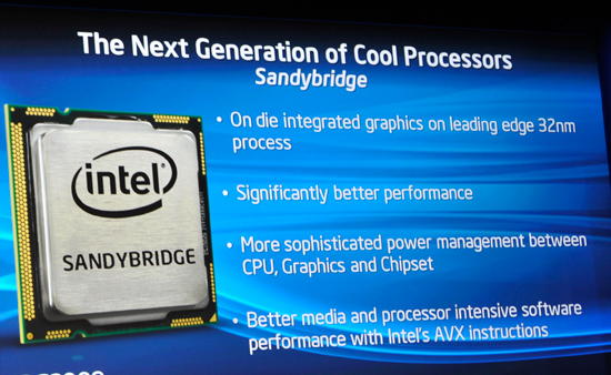
Both the CPU and GPU on SB will be able to turbo independently of one another. If you’re playing a game that uses more GPU than CPU, the CPU may run at stock speed (or lower) and the GPU can use the additional thermal headroom to clock up. The same applies in reverse if you’re running something computationally intensive.
On the CPU side little is known about the execution pipeline. Sandy Bridge enables support for AVX instructions, just like Bulldozer. The CPU will also have dedicated hardware video transcoding hardware to fend off advances by GPUs in the transcoding space.
Caches remain mostly unchanged. The L1 cache is still 64KB (32KB instruction + 32KB data) and the L2 is still a low latency 256KB. I measured both as still 4 and 10 cycles respectively. The L3 cache has changed however.
Only the Core i7 2600 has an 8MB L3 cache, the 2400, 2500 and 2600 have a 6MB L3 and the 2100 has a 3MB L3. The L3 size should matter more with Sandy Bridge due to the fact that it’s shared by the GPU in those cases where the integrated graphics is active. I am a bit puzzled why Intel strayed from the steadfast 2MB L3 per core Nehalem’s lead architect wanted to commit to. I guess I’ll find out more from him at IDF :)
The other change appears to either be L3 cache latency or prefetcher aggressiveness, or both. Although most third party tools don’t accurately measure L3 latency they can usually give you a rough idea of latency changes between similar architectures. In this case I turned to cachemem which reported Sandy Bridge’s L3 latency as 26 cycles, down from ~35 in Lynnfield (Lynnfield’s actual L3 latency is 42 clocks).
As I mentioned before, I’m not sure whether this is the result of a lower latency L3 cache or more aggressive prefetchers, or both. I had limited time with the system and was unfortunately unable to do much more.
And that’s about it. I can fit everything I know about Sandy Bridge onto a single page and even then it’s not telling us much. We’ll certainly find out more at IDF next month. What I will say is this: Sandy Bridge is not a minor update. As you’ll soon see, the performance improvements the CPU will offer across the board will make most anyone want to upgrade.


200 Comments
View All Comments
tatertot - Tuesday, August 31, 2010 - link
Can you also confirm whether or not the GPU turbo was also disabled?DanNeely - Saturday, August 28, 2010 - link
Do you think Intel will be sharing preliminary performance/pricing data on LGA 2011 by the time that the first LGA 1155 parts start shipping? I'm on 1366 now and would like to know if staying on the high end platform will be a reasonable option or if there isn't any point in holding off for another 6 months on my upgrade.Anand Lal Shimpi - Saturday, August 28, 2010 - link
I wouldn't expect any near-final LGA-2011 performance data until Q2 next year, well after the LGA-1155 launch.Take care,
Anand
Casper42 - Saturday, August 28, 2010 - link
2 things jumped out at me1) No USB3 - Major FAIL. Putting USB3 in an Intel chipset will drive huge adoption rates rather than this limping in BS by manufacturers today. Not to mention that for Hard Drives, USB2 has been a bottleneck for a long time whereas only top end SSDs today are maxing out SATA3
2) 2 chips with Quad Core and no HT that are identical except for Clock speed and one of them is essentially the 400 and the other is the 500? WTF? Call them the 2410, 2420, 2430, etc. That gives you like 8 or 9 speed bins for that family. Whomever is doing the numbering at Intel needs a swift kick to the head to get them back on track mentally as things just get more and more confusing. You have the i3/i5/i7 today, why not just change it to:
i2 = Dual Core no HT/Turbo
i3 = Dual Core with HT and/or Turbo
i4 = Quad Core no HT/Turbo
i5 = Quad WITH
i6 = Six without
etc
As it stands now we have i5 with both dual and quad core and i7 with 4 and 6. just doesnt make sense.
dertechie - Saturday, August 28, 2010 - link
That's quite the IPC improvement there. Not quite Netburst to Core 2 but a lot more than I expected (I was expecting something on the order of 5%, with most gains coming from ramping clocks with the extra headroom of 32nm).Question is, do I want the i5-2500K more than I loathe Intel's motherboard department? I'm seeing them bring out new sockets almost as often as new processor families, which really, really does not make me confident in the socket's future.
I will wait at least for Bulldozer benches before buying whatever makes sense at that time (okay, probably weighted in AMD's favor). I've lasted 4 years on this Pentium D, I can live another half of one.
IntelUser2000 - Saturday, August 28, 2010 - link
Why do some people still compare Netburst vs. Core 2? The Pentium 4 generation was a clock speed focused that that FAILED to realize its clock speed potential so it looked really bad compared to Core 2.Compared to Core Duo Core 2 was only 15-20% faster. Sandy Bridge manages to do another 20%, which is really good in a generation, yea?
ssj4Gogeta - Saturday, August 28, 2010 - link
Pentium D to SB will be such a huuuuge jump, lol.neslog - Saturday, August 28, 2010 - link
Your excellent article was exciting to read. Thank you!I noticed a small typo on the Windows 7 Gaming Performance page in the first line under the Data Recovery chart : "Clock for clock...to the i7{5} 760..."
ET - Saturday, August 28, 2010 - link
I think that the integrated graphics here are a game changer. Sure nobody will look to them for serious gaming, but finally they're at a point where if you buy any CPU you will be able to play most games, even if at low settings. I'll be looking forward especially to the mobile CPU's. With Bobcat around the corner, I guess next year we will finally see mainstreams notebooks become capable of some game playing, which will be great (and bad for NVIDIA).Exodite - Saturday, August 28, 2010 - link
What I'd like to see is something like Nvidia's Optimus make it to the desktop. With both AMD and Intel going for on-chip integrated graphics the market is practically begging for a unified standard for graphics switching.The next-generation IGPs look to be competent enough for anything but high-end gaming, which means I should be able to power down my discrete graphics card completely most of the time. The end result would be significant reductions in noise generation, power usage and heat emissions.
Having discreet graphics cards reduced to basically connector-less, slot-in cards for on-demand co-processing seems the logical step.