Everything You Always Wanted to Know About SDRAM (Memory): But Were Afraid to Ask
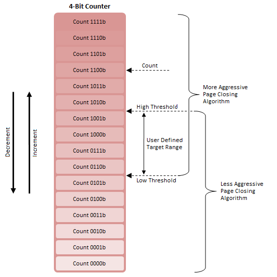
by Rajinder Gill on August 15, 2010 10:59 PM ESTFirst, consider a 4-bit counter with two adjustable thresholds (Figure 12). When Count is greater than High Threshold, Algorithm A is deemed appropriate; the same is true concerning Algorithm B and Count less than Low Threshold.
For the range between High Threshold and Low Threshold, either algorithm may be in effect. This is because a switch from Algorithm B to Algorithm A will occur only with Count greater than High Threshold and increasing and a switch from Algorithm A to Algorithm B will occur only with Count less than Low Threshold and decreasing.
The overlap range is also the Target Range as the system will naturally attempt to maintain Counter between these two points. This is true since Algorithm A tends to lower Count while Algorithm B tends to raise Count. This system acts to reduce or eliminate rapid thrashing between algorithms.
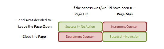
Next, define a truth table (Figure 13) defining how Count will vary. By doing so we can encode a feedback mechanism into our system. Successful predictions by the Adaptive Page Close Logic - a prevented page-miss access (good) in response to a decision to close a page or a facilitated page-hit access (good) in response to a decision to leave a page open - suggest no change to policy is required and so never modify Count.
For a facilitated page-miss access (bad) due to a poor decision to leave a page open, increment Count. If Count were to trend upward we could conceivably conclude that the current policy was most often wrong and not only that, tended to leave pages open far too long while "fishing" for page-hit operations. The current algorithm must not be closing pages aggressively enough.
For a prevented page-hit access (bad) due to a poor decision to close a page early, decrement Count. If Count were to trend downward we would suspect the opposite: the algorithm is too aggressively closing pages and leaving potential page-hits on the cutting room floor.
As best we can tell, this construct represent reality for APM Technology. Although we would like to believe the system has more than two gears (algorithms), our model perfectly explains the existing control register both in type and number.
Looking ahead you will see Max Page Close Limit and Min Page Close Limit are the specified High and Low Threshold values, respectively. Setting a larger difference increases the size of the feedback dead band, slowing the rate at which system responds to its own evaluative efforts. Mistake Counter is represented by the starting Count and should be set somewhere near the middle of the dead band.
Adaptive Timeout Counter sets the assertion time of any decision to keep a page open (i.e. how long before the decision to keep a page open stands before we give up hope of a page-hit access). Repeated access to the same page will reset this counter each time as long as the remaining lifetime is non-zero. Lower values result in a more aggressive page close policy and vice versa for higher values.
Request Rate, we believe, controls how often Count (Mistake Counter) is updated, and therefore how smoothly the system adapts to quickly changing workloads. There must be a good reason not to flippantly set this interrupt rate as low as possible. Perhaps this depletes hardware resources needed for other operations or maybe higher duty cycles disproportionally raises power consumption. Whatever the reason, there's more than a fair chance you can hurt performance if you're just spit-balling with this setting.


46 Comments
View All Comments
bowhe - Tuesday, October 26, 2010 - link
Thanks for these great articles!What I didn't understand yet:
You state "Installing more than one DIMM per channel does not double the Memory Bus bandwidth, as modules co-located in the same channel must compete for access to a shared 64-bit sub-bus; however, adding more modules does have the added benefit of doubling the number of pages that may be open concurrently (twice the ranks for twice the fun!)". This sounds very positive, but:
Some system manufacturers state that with 3 dimms the memory frequency can be for example 1333MHz, but with 6 dimms it needs to drop to 800MHz. Why does the frequency need to drop when using 6 versus 3 dimms? Does this apply to high end boards like the Gigabyte-X58A-UD9?
Some manufacturer states in a small side note of a 24GB kit (6x4GB) that the stated frequency/timing is only guaranteed when using 3 dimm slots. This leads me to think that any 3 dimms of the set can do the stated timing, but when all are used something inherent in the design or interaction of the i7 processor, motherboard and dimm prevents the use of stated frequency/timings? What is it?
Can one overcome these limitations by adjusting voltages in a high end board like the Gigabyte-X58A-UD9? (without use of extreme cooling <32F/0C)
Thanks a lot!
kakfjak - Thursday, May 5, 2011 - link
www.stylishdudes.com
All kinds of shoes + tide bag
Free transport
cochleoid - Tuesday, March 12, 2013 - link
"When associated in groups of two (DDR), four (DDR2) or eight (DDR3), these banks form the next higher logical unit, known as a rank. "This mislead me. DDR2 may have coincidentally introduced 3 bit banks - allowing for 8 bank chips - but a typical old SDRAM (no DDR) chip had 4 banks.
"We can now see why the DDR3 core has a 8n-prefetch (where n refers to the number of banks per rank) as every read access to the memory requires a minimum of 64 bits (8 bytes) of data to be transferred. This is because each bank, of which there are eight for DDR3, fetches no less than 8 bits (1 byte) of data per read request - the equivalent of one column's worth of data. Whether or not the system actually makes use of all 8 bytes of transferred data is irrelevant. Any delivered data not actually requested can be safely disregarded as it's just a copy of what is still retained in memory."
This threw me off even more. What's happening is that the data at 8 consecutive (or otherwise close, depending on the burst mode) column addresses is being bursted on each read. "n" refers to the width of the memory chip, or the size of the "word" at a particular column address. "n" does not have any relation to the number of banks in a rank.
8 8bit-wide DDR3 chips would make a total module width of 64 bits or 8 bytes at each column address. 8 column addresses would be 64 bytes (not 8 bytes, as the article seems to suggest), which actually corresponds to the cacheline size on most PCs.
SDRAM could burst in sizes of 1,2,4,8
DDR could burst in sizes of only 2,4,8
DDR2 could burst in sizes of only 4,8
DDR3 can burst only in 8.
(All of these could burst in 8, filling the 64 byte cachline in one read operation. The difference with the generations of DDR has been a larger minimum wait in interface clock cycles as the interface got faster and the row accesses remained sluggish.)
The internal clock of SDRAM has been limited by the speed of row accesses. What the 2n,4n,8n prefetches are doing is transferring more of this data available in an open row out at higher interface speeds with the rest of the system. It has nothing to do with the banks.
SDRAM chips were segmented into independently operating banks so that parallel operations on interleaved banks could be synchronized or pipelined. 2n, 4n, and 8n prefetch buffering can be applied without independently operating banks.
ricardo_sa - Saturday, March 26, 2016 - link
Thanks for the detailed explanation. You really saved my day. Ive read this article some time ago to help me understand how a DDR3 worked (theres few detailed explanations on google) and it turned out to be the worst mistake possible. I got the concepts wrong because of the incompetence of the publisher and lost a lot of time dealing with that 8 Bank misconception about the 64 bits.So it turns out one can only write a burst at 1 bank at a time, am i right? Otherwise you could access all the 8 banks in one single write/read....
Huendli - Friday, March 13, 2015 - link
Thanks for this interesting read with much attention to detail!"a top priority [...] should be to focus development on reducing absolute minimum latency requirements for timings such as CAS and tRCD, rather than chasing raw synthetic bandwidth figures or setting outright frequency records at the expense of unduly high random access times."
The latter's exactly what happened. DDR3-1600 modules with CL7 timings were widely available at the time this article had been written. Nowadays, you only get ridiculously-named bars with equally-ridiculously monstrous heatspreaders, but more bandwidth and worse timings than ever.
Anuradha - Tuesday, March 9, 2021 - link
Each rank consists of 8 banks, OR, each rank consists of 8 ICs and each IC consists of 8 banks??