Everything You Always Wanted to Know About SDRAM (Memory): But Were Afraid to Ask
by Rajinder Gill on August 15, 2010 10:59 PM ESTHere at AnandTech we decided to go the extra mile for you, our loyal reader. A few weeks back we approached ASUS USA Tech Support with a request to set-up a technical consultation with their Firmware Engineering Department. After passing along our request, what came out of the meeting was a special beta BIOS that added a number of previously unavailable memory tuning registers once excluded from direct user control.
In the interest of full disclosure, we did request the same help from EVGA and although they were willing to back our play, technical difficulties prevented them from delivering everything we had originally hoped for.
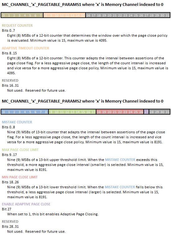
Seen below, these new registers are: Adaptive Page Closing, Adaptive Timeout Counter, Request Counter, Max Page Close Limit, Min Page Close Limit, and Mistake Counter. As suspected, the first setting is used to enabled or disable the feature entirely. Interesting enough, Intel chose not to enable this feature by default; so we leave it up to you.
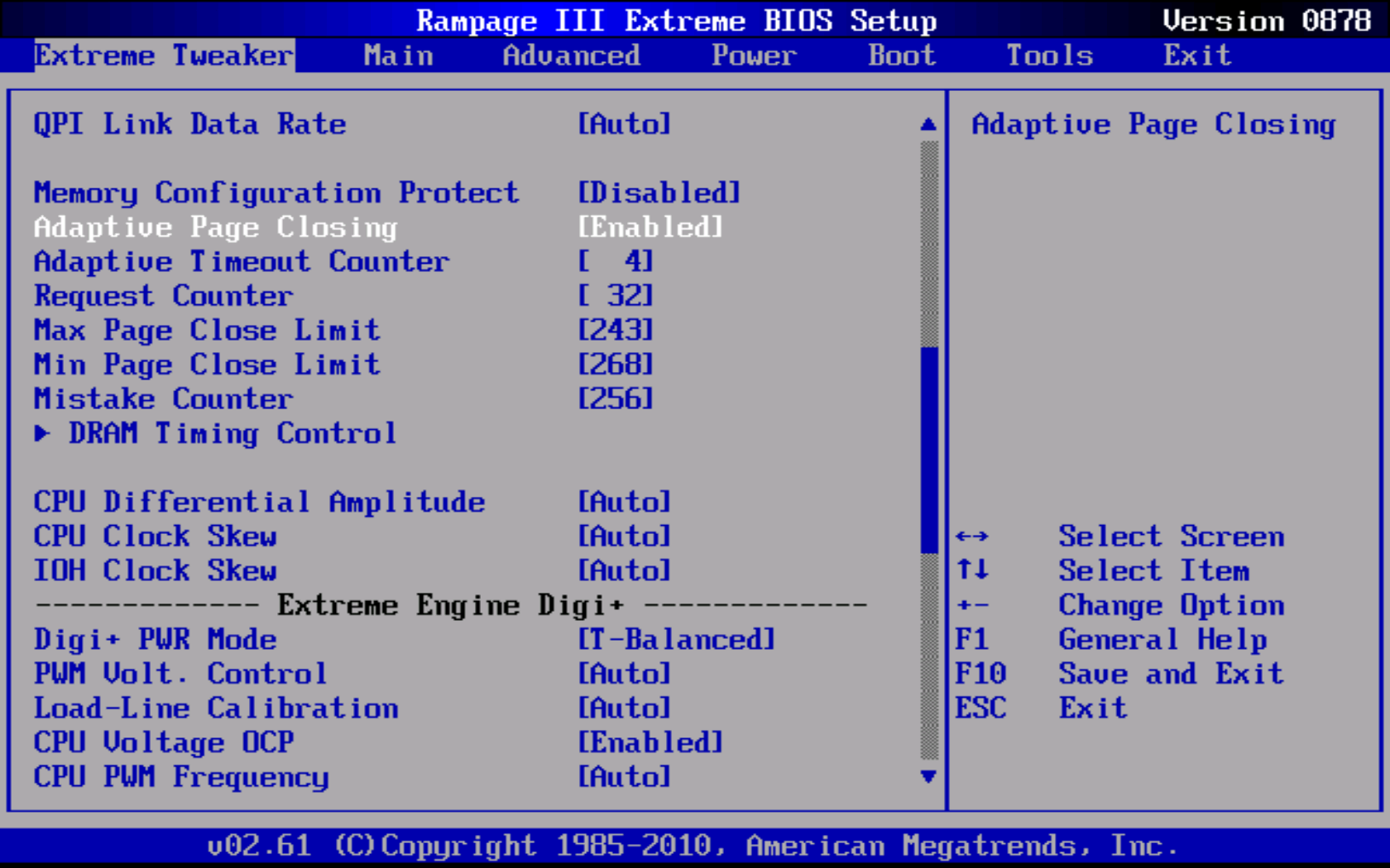
Click to enlarge
A short description of each register is shown below (taken from Intel Core i7-900 Desktop Processor Extreme Edition Series and Intel Core i7-900 Desktop Processor Series Datasheet, Volume 2, page 79, dated October 2009). Be aware the source most likely contains at least one known error. In particular, Intel has provided exactly the same description for Adaptive Timeout Counter and Mistake Counter. As well, the bit count for Mistake Counter in the table does not match the value in the text, further suggesting someone goofed.
Once you've had time to fully digest the information above - and ponder how awesome we are - we would like to cordially invite you to do some of your own testing and report your results at our forums. AnandTech readers with a valid login can download ASUS Rampage III Extreme BIOS release 0878 now. We haven't really had a chance to do any significant experimenting with what little spare time we have and we need your help exploring uncharted territory...


46 Comments
View All Comments
JarredWalton - Monday, August 16, 2010 - link
Oh, it's missing a lot more than just voltage information. :-) There are rebates on most memory kits right now, for instance. Still, I felt it was useful to highlight where the current "best deals" tend to fall.I personally wouldn't touch the ultra-expensive $150+ stuff, but up to $115 has potential at least. For a lower voltage kit, G.Skill has an ECO line rated at DDR3-1600 7-8-7-24-2N and 1.35V for $103. Worth a look at least....
JarredWalton - Monday, August 16, 2010 - link
Note: I screwed up my table above. DDR3 is two bits per clock, so the base clocks are all twice what I listed, which means latency for CAS is half what I listed. Sorry. Got things confused with GDDR5. :-) The relative latency is still the same, of course, which is the main point.JarredWalton - Monday, August 16, 2010 - link
Side note number two: And of course, CAS Latency isn't the be-all, end-all. According to benchmarks by Raja, DDR3-2000 at 6-9-6 timings often trails RAM at 7-8-7, as the tRCD difference becomes more pronounced in some cases.Rajinder Gill - Monday, August 16, 2010 - link
Sorry I should have said 7-7-8 vs 6-9-8. This happens when the number of random access requests are high (fewer back to back reads). Benchmarks like WinRar and Super Pi (synthetic) are mainly the ones that show this.-Raja
Drag0nFire - Friday, August 20, 2010 - link
I've had great experience with the ECO line. Put the 2x2 kit you mentioned in two computers so far, and it's been great. Feels like a steal to get such high speed and low voltage at such a great price.kalniel - Monday, August 16, 2010 - link
Thanks for taking the time to write the article - the cycle time-line figures are very helpful, but I'm struggling to understand it correctly.Take fig. 5. There doesn't seem to be a Read to Precharge Delay. If we follow the recommendation of CL+tBurst = tRCP + tRP then won't there be a delay of 4T after the Data Read Burst before the RAS Precharge starts, giving a Row Cycle Time of 26 rather than 24?
kjboughton - Monday, August 16, 2010 - link
tRTP may very well be 4T but the minimum RAS Active Time (tRAS) is 18T. The precharge is precluded from occuring until this period has expired making the clock at T + 18 the first opportunity to precharge the bank. Add to this the RAS Precharge (tRP) and you have the Row Cycle Time (tRC = tRAS + tRP) - the minimum time any single row MUST remain open before it can be closed (and before another page in the same bank can be accessed).Does this help?
kalniel - Monday, August 16, 2010 - link
I thought the Read to Precharge Delay was there precisely to ensure you waited the minimum RAS active time before precharging the bank. Are you saying that the tRTP doesn't apply if you've already finished tRCD+CL+tBurst within tRAS so can start precharging as soon as minimum RAS active time is achieved?In other words, tRTP doesn't have a bearing on a single burst per page, but is there to help synchronise auto-precharge reads within the same page?
My ignorance may be beyond redemption!
kjboughton - Monday, August 16, 2010 - link
Read to Precharge Delay (tRTP) is the minimum wait time from a READ (column access) to bank PRECHARGE.RAS Active Time (tRAS) is the minimum wait time from an ACTIVATE (row access) to bank PRECHARGE.
Both times must be satisfied before the bank can be precharged. Perhaps I wasn't quite clear enough on this point. I hope this clears things up.
kalniel - Monday, August 16, 2010 - link
I think I've got it now, thanks. My brain saw the relevant diagram and screamed 'Cthulu' instead.