One thing that specifically sets MSI’s G210 card apart from the others is that it comes packed with more than the bare minimum as is usually found with cards at this price level. In terms of included hardware you don’t get anything besides the card, the manual, the brackets, and the software – but it’s the software that makes the difference here.
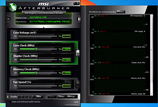
MSI offers several software utilities for all of their cards, and the cornerstone of this is their Afterburner software. In a nutshell Afterburner is the distilled child of the long-favored RivaTuner utility, using RivaTuner’s technology to offer a straightforward video card overclocking and monitoring tool. We’ll be looking at Afterburner and other overclocking utilities in-depth later this month, but we wanted to take a quick look at it today.
As a RivaTuner descendant, Afterburner offers overclocking of the core, shader, and memory clocks, along with the usual suite of clock and temperature monitoring. Furthermore despite being an MSI utility, it works on a generic level with all NVIDIA and AMD GPUs that Afterburner supports. As a trump card specifically for MSI’s cards, it’s also capable of doing voltage tweaking on most of their cards. In the case of the G210 however, this feature is not supported (which would be a bad idea anyhow since it’s passively cooled).
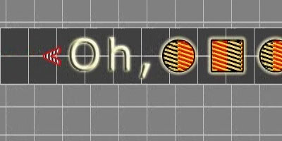
Finally, we took a look at the G210’s usability in an HTPC setting. With the same VP4 decoder and 8-channel LPCM audio capabilities as on the rest of NVIDIA’s 40nm G(T) 200 series, the G210 has the potential to be a solid HTPC card on paper. As with the other low-profile cards we’ve been looking at this month, we ran it through the Cheese Slices HD deinterlacing test, which as we’ve seen can quickly expose any flaws or limitations in a card’s video decoding and post-processing capabilities
Unfortunately the G210 did extremely poorly here. In our testing the G210 would consistently drop frames when trying to run the Cheese Slices test, leading to it only processing around 2 out of every 3 frames. NVIDIA doesn’t offer any deinterlacing settings beyond enabling/disabling Inverse Telecine support, so the interlacing method used here is whatever the card/drivers support, which looks to be an attempt at Vector Adaptive deinterlacing.

GeForce 210

GeForce GT 220
The quality is reminiscent of VA deinterlacing, however it’s not as clean as what we’ve seen on the GT 220. More to the point, the G210 clearly doesn’t have the processing power to do this, but it’s unable to fall back to a lesser mode. Cheese Slices isn’t a fair test by any means, but it does mean something when a card can’t gracefully fail the test. Once we throw deinterlacing out of the equation however the G210 has no problem playing back progressively encoded MPEG-2 and H.264 material. It looks to only be serious limited when deinterlacing, which means the G210 is only at a serious disadvantage with interlaced material such as live television.


24 Comments
View All Comments
hwhacker - Tuesday, February 16, 2010 - link
Hmm, maybe he knows something we don't?Last I heard circulating AMD was going to get (sample?) product from both TSMC and GF on 32nm, but that got all borked when TSMC cancelled 32nm. As such, now they will transition to each company's respective 28nm process instead. This is said to have messed up Northern Islands' release, but may result in a better (not just smaller/faster) product. Who knows if that's true. All things being equal, I'm sure AMD would like to use 28nm bulk at GF.
As for nVIDIA, it's been interesting to watch. First they said absolutely not to GF, then 40nm at TSMC happened. After that Jensen was said to be in talks with GF, publically said some good things about GF over TSMC (likely because they're angry about 40nm RE: Fermi and used it for intimidation) and that's all we know. All things being equal, I'm sure nVIDIA would like to use 28nm bulk at TSMC.
Natfly - Tuesday, February 16, 2010 - link
You're right, both companies canned their 32nm bulk processes. So either the author is insinuating that nVidia is going to switch to 32nm SOI or he means 28nm.Ryan Smith - Tuesday, February 16, 2010 - link
He means 28nm.Natfly - Tuesday, February 16, 2010 - link
My apologies, I would have referred to you by name if I wasn't too lazy to go back to the article from the comments page to check :P