The RV870 Story: AMD Showing up to the Fight
by Anand Lal Shimpi on February 14, 2010 12:00 AM EST- Posted in
- GPUs
Process vs. Architecture: The Difference Between ATI and NVIDIA
Ever since NV30 (GeForce FX), NVIDIA hasn’t been first to transition to any new manufacturing process. Instead of dedicating engineers to process technology, NVIDIA chooses to put more of its resources into architecture design. The flipside is true at ATI. ATI is much less afraid of new process nodes and thus devotes more engineering resources to manufacturing. Neither approach is the right one, they both have their tradeoffs.
NVIDIA’s approach means that on a mature process, it can execute frustratingly well. It also means that between major process boundaries (e.g. 55nm to 40nm), NVIDIA won’t be as competitive so it needs to spend more time to make its architecture more competitive. And you can do a lot with just architecture alone. Most of the effort put into RV770 was architecture and look at what it gave ATI compared to the RV670.
NVIDIA has historically believed it should let ATI take all of the risk jumping to a new process. Once the process is mature, NVIDIA would switch over. That’s great for NVIDIA, but it does mean that when it comes to jumping to a brand new process - ATI has more experience. Because ATI puts itself in this situation of having to jump to an unproven process earlier than its competitor, ATI has to dedicate more engineers to process technology in order to mitigate the risk.
In talking to me Carrell was quick to point out that moving between manufacturing processes is not a transition. A transition implies a smooth gradient from one technology to another. But moving between any major transistor nodes (e.g. 55nm to 45nm, not 90nm to 80nm) it’s less of a transition and more of a jump. You try to prepare for the jump, you try your best to land exactly where you want to, but once your feet leave the ground there’s very little to control where you end up.
Any process node jump involves a great deal of risk. The trick as a semiconductor manufacturer is how you minimize that risk.
At some point, both manufacturers have to build chips on a new process node otherwise they run the risk of becoming obsolete. If you’re more than one process generation behind, it’s game over for you. The question is, what type of chip do you build on a brand new process?
There are two schools of thought here: big jump or little jump. The size refers to the size of the chip you’re using in the jump.
Proponents of the little jump believe the following. In a new process, the defect density (number of defects per unit area on the wafer) isn’t very good. You’ll have a high number defects spread out all over the wafer. In order to minimize the impact of high defect density, you should use a little die.
If we have a wafer that has 100 defects across the surface of the wafer and can fit 1000 die on the wafer, the chance that any one die will be hit with a defect is only 10%.
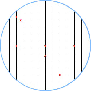
A hypothetical wafer with 7 defects and a small die. Individual die are less likely to be impacted by defects.
The big jump is naturally the opposite. You use a big die on the new process. Now instead of 1000 die sharing 100 defects, you might only have 200 die sharing 100 defects. If there’s an even distribution of defects (which isn’t how it works), the chance of a die being hit with a defect is now 50%.
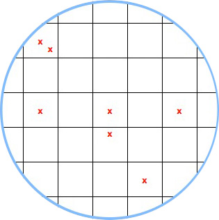
A hypothetical wafer with 7 defects and a large die.
Based on yields alone, there’s no reason you’d ever want to do a big jump. But there is good to be had from the big jump approach.
The obvious reason to do a big jump is if the things you’re going to be able to do by making huge chips (e.g. outperform the competition) will net you more revenue than if you had more of a smaller chip.
The not so obvious, but even more important reason to do a big jump is actually the reason most don’t like the big jump philosophy. Larger die are more likely to expose process problems because they will fail more often. With more opportunity to fail, you get more opportunity to see shortcomings in the process early on.
This is risky to your product, but it gives you a lot of learning that you can then use for future products based on the same process.


132 Comments
View All Comments
AdiQue - Sunday, February 14, 2010 - link
I fully subscribe to point raised by a few previous posters. Namely, the article being such a worthy read, it actually justifies the creation of an account for the sheer reason of expressing appreciation to your fantastic work, which does stand out in the otherwise well saturated market of technology blogs.geok1ng - Sunday, February 14, 2010 - link
"I almost wonder if AMD’s CPU team could learn from the graphics group's execution. I do hope that along with the ATI acquisition came the open mindedness to learn from one another"it would be a true concern if based on mere observation, but the hard facts are soo much terrible: AMD fired tons of ATI personnel, hence ATI drivers are years behind NVIDIA- we are still begging for centered timings on ATO cards, a feature that NVIDIA offers 6 generations past! ATI produces cards that are gameless. DirectX 10.1?! There was a single game with DirectX 10.1 support, and NVIDIA made the game developer REMOVE DirectX 10.1 features with a game patch that "increased" performance. DirectX 11?! ATI has to put money on driver developing team and spend TONS of cash in game developing.
I would be a happier costumer if the raw performance of my 4870X2 was paired with the seamless driver experience of my previous 8800GT.
And another game that AMD was too late is the netbook and ultralow voltage mobile market. A company with the expertise in integrated graphics and HTPCs GPUs with ZERO market share on this segment?! give me a break!
LordanSS - Monday, February 15, 2010 - link
Funny... after the heaps of problems I had with drivers, stability and whatnot with my old 8800GTS (the original one, 320MB), I decided to switch to ATI with a 4870. Don't regret doing that.My only gripe with my current 5870 is the drivers' and the stupid giant mouse cursor. The Catalyst 9.12 hotfix got rid of it, but it came back on the 10.1.... go figure. Other than that, haven't had problems with it and have been getting great performance.
blackbrrd - Monday, February 15, 2010 - link
I think the reason he had issues with the X2 is that it's a dual card. I think most gfx card driver problems comes from dual cards in any configuration (dual, crossfire, sli)The reason you had issues with the 320mb card is that it had some real issues because of the half-memory. The 320mb cards where cards originally intended as gtx cards, but binned as gts cards that again got binned as 320mb cards instead of 640mb cards. Somehow Nvidia didn't test these cards good enough.
RJohnson - Sunday, February 14, 2010 - link
Please get back under your bridge troll...Warren21 - Sunday, February 14, 2010 - link
Are you kidding me? Become informed before you spread FUD like this. I've been able to choose centered timings in my CCC since I've had my 2900 Pro back in fall 2007. Even today on my CrossFire setup you can still use it.As for your DX10.1 statement, thank NVIDIA for that. You must remember that THEY are the 600lb gorilla of the graphics industry - I fail to see how the exact instance you cite does anything other than prove just that.
As for the DX11 statement, if NVIDIA had it today I bet you'd be singing a different tune. The fact that it's here today is because of Microsoft's schedule which both ATI and NVIDIA follow. NV would have liked nothing more than to have Fermi out in 2009, believe that.
Kjella - Sunday, February 14, 2010 - link
"AMD fired tons of ATI personnel, hence ATI drivers are years behind NVIDIA-"Wow, you got it backwards. The old ATI drivers sucked horribly, they may not be great now either but whatever AMD did or didn't do the drivers have been getting better, not worse.
Scali - Sunday, February 14, 2010 - link
It's a shame that AMD doesn't have its driver department firing on all cylinders like the hardware department is.The 5000-series are still plagued with various annoying bugs, such as the video playback issues you discovered, and the 'gray screen' bug under Windows 7.
Then there's OpenCL, which still hasn't made it into a release driver yet (while nVidia has been winning over many developers with Cuda and PhysX in the meantine, while also offering OpenCL support in release drivers, which support a wider set of features than AMD, and better performance).
And through the months that I've had my 5770 I've noticed various rendering glitches aswell, although most of them seem to have been solved with later driver updates.
And that's just the Windows side. Linux and OS X aren't doing all that great either. FreeBSD isn't even supported at all.
hwhacker - Sunday, February 14, 2010 - link
I don't log in and comment very often, but had to for this article.Anand, these type of articles (Rv770,'Rv870',and SSD) are beyond awesome. I hope it continues for Northern Islands and beyond. Everything from the RV870 jar tidbit to the original die spec to the SunSpotting info. It's great that AMD/ATi allows you to report this information, and that you have the journalistic chops to inquire/write about it. Can not provide enough praise. I hope Kendell and his colleagues (like Henri Richard) continue this awesome 'engineering honesty' PR into the future. The more they share, within understandable reason, the more I believe a person can trust a company and therefore support it.
I love the little dropped hints BTW. Was R600 supposed to be 65nm but early TSMC problems cause it revert to 80nm like was rumored? Was Cypress originally planned as ~1920 shaders (2000?) with a 384-bit bus? Would sideport have helped the scaling issues with Hemlock? I don't know these answers, but the fact all of these things were indirectly addressed (without upsetting AMD) is great to see explored, as it affirms my belief I'm not the only one interested in them. It's great to learn the informed why, not just the unsubstantiated what.
If I may preemptively pose an inquiry, please ask whomever at AMD when NI is briefed if TSMC canceling their 32nm node and moving straight to 28nm had anything to do with redesigns of that chip. There are rumors it caused them to rethink what the largest chip should be, and perhaps revert back to what the original Cypress design (as hinted in this article?) for that chip, causing a delay from Q2-Q3 to Q3-Q4, not unlike the 30-45 day window you mention about redesigning Cypress. I wonder if NI was originally meant to be a straight shrink?
hwhacker - Sunday, February 14, 2010 - link
I meant Carrell above. Not quite sure why I wrote Kendell.