The RV870 Story: AMD Showing up to the Fight
by Anand Lal Shimpi on February 14, 2010 12:00 AM EST- Posted in
- GPUs
The Cost of Jumping to 40nm
This part of the story could almost stand on its own, but it directly impacts much of what happened with Cypress and the entire Evergreen stack that it’s worth talking about here.
By now you’ve most likely heard about issues with TSMC’s 40nm process. While the word is that the issues are finally over, poor yields and a slower than expected ramp lead to Cypress shortages last year and contributed to NVIDIA’s Fermi/GF100 delay. For the next couple of pages I want to talk about the move to 40nm and why it’s been so difficult.
The biggest issue with being a fabless semiconductor is that you have one more vendor to deal with when you’re trying to get out a new product. On top of dealing with memory companies, component manufacturers and folks who have IP you need, you also have to deal with a third party that’s going to actually make your chip. To make matters worse, every year or so, your foundry partner comes to you with a brand new process to use.
The pitch always goes the same way. This new process is usually a lot smaller, can run faster and uses less power. As with any company whose job it is to sell something, your foundry partner wants you to buy its latest and greatest as soon as possible. And as is usually the case in the PC industry, they want you to buy it before it's actually ready.
But have no fear. What normally happens is your foundry company will come to you with a list of design rules and hints. If you follow all of the guidelines, the foundry will guarantee that they can produce your chip and that it will work. In other words, do what we tell you to do, and your chip will yield.
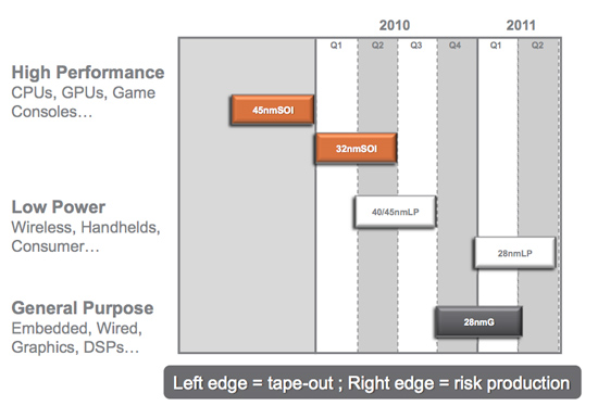
Global Foundries' 2010 - 2011 Manufacturing Roadmap
The problem is that if you follow every last one of these design rules and hints your chip won’t be any faster than it was on the older manufacturing process. Your yield will be about the same but your cost will be higher since you’ll bloat your design taking into account these “hints”.
Generally between process nodes the size of the wafer doesn’t change. We were at 200mm wafers for a while and now modern fabs use 300mm wafers. The transistor size does shrink however, so in theory you could fit more die on a wafer with each process shrink.
The problem is with any new process, the cost per wafer goes up. It’s a new process, most likely more complex, and thus the wafer cost is higher. If the wafer costs are 50% higher, then you need to fit at least 50% more die on each wafer in order to break even with your costs on the old process. In reality you actually need to fit more than 50% die per wafer on the new process because yields usually suck at the start. But if you follow the foundry’s guidelines to guarantee yield, you won’t even be close to breaking even.
The end result is you get zero benefit from moving to the new process. That’s not an option for anyone looking to actually use Moore’s Law to their advantage. Definitely not for a GPU company.
The solution is to have some very smart people in your company that can take these design rules and hints the foundry provides, and figure out which ones can be ignored, and ways to work around the others. This is an area where ATI and NVIDIA differ greatly.


132 Comments
View All Comments
n7 - Sunday, February 14, 2010 - link
Another great story told.Thanx, Anand.
MrK6 - Sunday, February 14, 2010 - link
What a great piece. Thank you for taking the time to put this together; it's one of the best tech articles I've read.archcommus - Sunday, February 14, 2010 - link
Haven't even read the whole thing yet but I can already say this is excellent. Thank you, Anand.indicator - Sunday, February 14, 2010 - link
Hi allI felt I had to register here after reading this article , what a fantastic insight into everything that goes into making these GPU's and the dedication and talent it takes to be so creative.
Great to see Anands enthusiasm for the industry come across in the article too
I've been coming here and reading Anandtech since around the mid ninties I guess , it is a superb source of information , I look forward to every new article/review posted.
Keep it up guys
Lee
(uk)
d3x7r0 - Sunday, February 14, 2010 - link
Very very good article as usual in this website. AnandTech has been one of my favourite sites in the area for so long I don't even remember how I found out about the website, I actually believe I was still in 56k when I first came here.Anyway reading this article made me speculate on something (and please correct me if I'm wrong): If I got the timings right AMD-ATI should be working on the Northern Islands since the Radeon HD4xxx series days so the same issues they had with the HD5xxx series would be in the past. If this is true it means they know the HD4xxx were a success from the beginning of the process (or near it) and as such I can't but help it be even more excited to see what the next generation of ATI cards has in store.
It's such a good time to be an ATI fan it's not even funny :D
Atlantis6000bc - Sunday, February 14, 2010 - link
Those kind of article are the prime reason why I keep coming back to Anand....keep 'em comingThe13thWizard - Sunday, February 14, 2010 - link
Thanks Anand! Thats the best IT article Ive ever read! Very toughtfull and interesting!arnavvdesai - Sunday, February 14, 2010 - link
Really helps understand the industry a lot more. I really wish AMD would take a cue from its graphics division and really start hammering out what kind of chips do they want to build. However, they have their own set of challenges as Intel unlike NVIDIA is really really good on the foundry side as well.However, with gaming becoming more and more centered on consoles, does ATi have something cooking for the next generation of consoles? Would love Anand to ask them something about that. Do they believe that they will continue to sell enough cards to continue recouping their costs of designing and manufacturing them.
Vishnu Narayanan S - Sunday, February 14, 2010 - link
First of all, hats off to you for this amazing article.... Its these articles that bind us to the Anandtech website for years and years.I sincerely hope and request you to provide similar in-depth and "behind the scenes" stories from NVIDIA and Intel. Just to satisfy the FANbois... lol
fausto412 - Sunday, February 14, 2010 - link
once i started reading i couldn't stop. for a geek like me this was almost like sex:) keep them coming!