The RV870 Story: AMD Showing up to the Fight
by Anand Lal Shimpi on February 14, 2010 12:00 AM EST- Posted in
- GPUs
Adjusting Trajectory & Slipping Schedule
Carrell didn’t believe in building big chips anymore. It wasn’t that it was too difficult, it’s that it took too long for a $600 GPU to turn into a $200 GPU. AMD believed that the most important market was the larger (both in quantity and revenue) performance mainstream segment.
Rather than making the $200 - $300 market wait for new technology, Carrell wanted to deliver it there first and then scale up/down to later address more expensive/cheaper markets.
The risk in RV770 was architecture and memory technology. The risk in RV870 was architecture and manufacturing process, the latter which was completely out of AMD’s control.
Early on Carrell believed that TSMC’s 40nm wasn’t mature enough and that when it was ready, its cost was going to be much higher than expected. While he didn’t elaborate on this at the time, Carrell told me that there was a lot of information tuning that made TSMC’s 40nm look cheaper than it ended up being. I'll touch on this more later on in the article.
Carrell reluctantly went along with the desire to build a 400+ mm2 RV870 because he believed that when engineering wakes up and realizes that this isn’t going to be cheap, they’d be having another discussion.
In early 2008, going into Februrary, TSMC started dropping hints that ATI might not want to be so aggressive on what they think 40nm is going to cost. ATI’s costs might have been, at the time, a little optimistic.
Engineering came back and said that RV870 was going to be pretty expensive and suggested looking at the configuration a second time.
Which is exactly what they did.
The team met and stuck with Rick Bergman’s compromise: the GPU had to be at least 2x RV770, but the die size had to come down. ATI changed the configuration for Cypress (high end, single GPU RV870) in March of 2008.
And here’s where the new ATI really showed itself. We had a company that had decided to both 1) not let schedule slip, and 2) stop designing the biggest GPU possible. Yet in order to preserve the second belief, it had to sacrifice the first.
You have to understand, changing a chip configuration that late in the game, 1.5 years before launch, screws everything up. By the time RV770 came out, 870 was set in stone. Any changes even a year prior to that resets a lot of clocks. You have to go back and redo floorplan and configuration, there’s a lot of adjusting that happens. It takes at least a couple of weeks, sometimes a couple of months. It impacted schedule. And ATI had to work extremely hard to minimize that where possible. The Radeon HD 5870 was around 30 - 45 days late because of this change.
Remember ATI’s nothing-messes-with-schedule policy? It took a lot of guts on the part of the engineering team and Rick Bergman to accept a month+ hit on redesigning RV870. If you don’t show up to the fight, you lose by default, and that’s exactly what ATI was risking by agreeing to a redesign of Cypress.
This is also super important to understand, because it implies that at some point, NVIDIA made a conscious decision to be late with Fermi. ATI wasn’t the only one to know when DX11/Windows 7 were coming. NVIDIA was well aware and prioritized features that delayed Fermi rather than align with this market bulge. GPUs don’t get delayed without forewarning. AMD risked being late in order to make a smaller chip, NVIDIA risked being late to make a bigger one. These two companies are diverging.
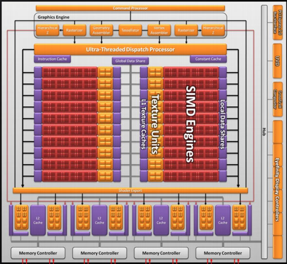
The actual RV870
Engineering was scrambling. RV870 had to be a lot smaller yet still deliver 2x the computational power of RV770. Features had to go.


132 Comments
View All Comments
Dudler - Sunday, February 14, 2010 - link
Whoa... Just Whoa.Very insightful and interesting.
Amd moving to GF next generation and Norther Islands this year?
Whoa.
Thx Anand :)
carlhenry - Sunday, February 14, 2010 - link
i really loved the eyefinity being so 'mission impossible'. awesome article!Patrick Wolf - Sunday, February 14, 2010 - link
The first rule of SunSpot: You don't talk about SunSpot. :Dmubeen - Tuesday, February 16, 2010 - link
Such an informative article Mr. Anand. Really appreciate your efforts.just4U - Tuesday, February 16, 2010 - link
I agree it's a great article, nice to see these ones pop up from time to time. It don't really matter to me if it's nvidia, amd or intel.. just having a more insightful read is refreshing.DearSX - Sunday, February 14, 2010 - link
I really do a like article like this. I wonder how old others are cause I'm 25 and I did not even notice how much reading things like this mattered. Its more important than buying something or performance figures imo.Paulman - Sunday, February 14, 2010 - link
I, too, will second that. Really cool. :PMrSpadge - Sunday, February 14, 2010 - link
Many thanks for this interesting article and especially the in-dpeth information about TSMC, the process and how ATI deals with it. Thanks to you, Anand, for writing it and thanks to the good guys at AMD for sharing this information!Beyond excellence :)
hyvonen - Monday, February 15, 2010 - link
And NVidia's call for "zero defects, zero variability" was jaw-dropping. Do they have any idea how silicon is manufactured?Unbelievable cluelessness... with this attitude, they are out of business in the next two years. They are completely unprepared to harness the potential in the latest process nodes.
Meanwhile, it also sounds like TSMC is way over its head in this - uncharacteristic screw-ups with the chamber matching, bad leakage etc. Not to mention the choice to delay HKMG until 28nm (and having to kill 32nm because of that). GF is going to eat them for lunch, and take over the foundry business.
ET - Sunday, February 14, 2010 - link
Indeed. One of the more interesting articles I've read in a while.