The RV870 Story: AMD Showing up to the Fight
by Anand Lal Shimpi on February 14, 2010 12:00 AM EST- Posted in
- GPUs
Process vs. Architecture: The Difference Between ATI and NVIDIA
Ever since NV30 (GeForce FX), NVIDIA hasn’t been first to transition to any new manufacturing process. Instead of dedicating engineers to process technology, NVIDIA chooses to put more of its resources into architecture design. The flipside is true at ATI. ATI is much less afraid of new process nodes and thus devotes more engineering resources to manufacturing. Neither approach is the right one, they both have their tradeoffs.
NVIDIA’s approach means that on a mature process, it can execute frustratingly well. It also means that between major process boundaries (e.g. 55nm to 40nm), NVIDIA won’t be as competitive so it needs to spend more time to make its architecture more competitive. And you can do a lot with just architecture alone. Most of the effort put into RV770 was architecture and look at what it gave ATI compared to the RV670.
NVIDIA has historically believed it should let ATI take all of the risk jumping to a new process. Once the process is mature, NVIDIA would switch over. That’s great for NVIDIA, but it does mean that when it comes to jumping to a brand new process - ATI has more experience. Because ATI puts itself in this situation of having to jump to an unproven process earlier than its competitor, ATI has to dedicate more engineers to process technology in order to mitigate the risk.
In talking to me Carrell was quick to point out that moving between manufacturing processes is not a transition. A transition implies a smooth gradient from one technology to another. But moving between any major transistor nodes (e.g. 55nm to 45nm, not 90nm to 80nm) it’s less of a transition and more of a jump. You try to prepare for the jump, you try your best to land exactly where you want to, but once your feet leave the ground there’s very little to control where you end up.
Any process node jump involves a great deal of risk. The trick as a semiconductor manufacturer is how you minimize that risk.
At some point, both manufacturers have to build chips on a new process node otherwise they run the risk of becoming obsolete. If you’re more than one process generation behind, it’s game over for you. The question is, what type of chip do you build on a brand new process?
There are two schools of thought here: big jump or little jump. The size refers to the size of the chip you’re using in the jump.
Proponents of the little jump believe the following. In a new process, the defect density (number of defects per unit area on the wafer) isn’t very good. You’ll have a high number defects spread out all over the wafer. In order to minimize the impact of high defect density, you should use a little die.
If we have a wafer that has 100 defects across the surface of the wafer and can fit 1000 die on the wafer, the chance that any one die will be hit with a defect is only 10%.
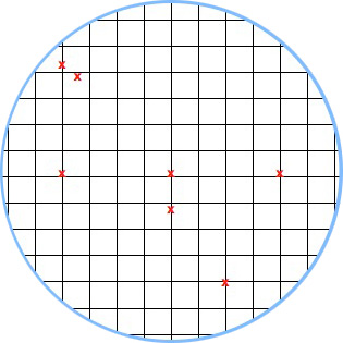
A hypothetical wafer with 7 defects and a small die. Individual die are less likely to be impacted by defects.
The big jump is naturally the opposite. You use a big die on the new process. Now instead of 1000 die sharing 100 defects, you might only have 200 die sharing 100 defects. If there’s an even distribution of defects (which isn’t how it works), the chance of a die being hit with a defect is now 50%.
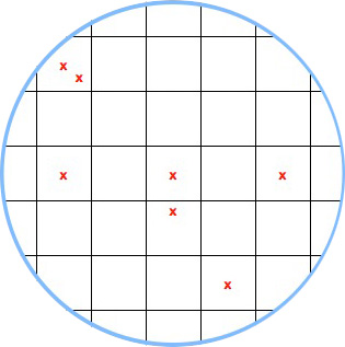
A hypothetical wafer with 7 defects and a large die.
Based on yields alone, there’s no reason you’d ever want to do a big jump. But there is good to be had from the big jump approach.
The obvious reason to do a big jump is if the things you’re going to be able to do by making huge chips (e.g. outperform the competition) will net you more revenue than if you had more of a smaller chip.
The not so obvious, but even more important reason to do a big jump is actually the reason most don’t like the big jump philosophy. Larger die are more likely to expose process problems because they will fail more often. With more opportunity to fail, you get more opportunity to see shortcomings in the process early on.
This is risky to your product, but it gives you a lot of learning that you can then use for future products based on the same process.


132 Comments
View All Comments
wlee15 - Sunday, February 14, 2010 - link
The USS Hornet is a carrier not a battleship.For shame Anand For Shame!
Anand Lal Shimpi - Monday, February 15, 2010 - link
wow - you're totally right, I can't believe I made that mistake. Looks like Ryan or Jarred caught it shortly after it went live though, whew :)And yes, for the record, I know the difference between an aircraft carrier and a battleship :)
Take care,
Anand
just4U - Tuesday, February 16, 2010 - link
LIES!!!!(hah)
Sahrin - Sunday, February 14, 2010 - link
Thank you - I was worried I'd be the only one to point this one out.Thank you Anand! This stuff is incredible. Just a few weeks ago I was looking back on the RV770 article and wishing it could be done again.
Kudos as well are due to AMD's PR guys - for having the courage to let the engineers sit down with the press, instead of needing to be there as minders. I guarantee you that every single time, the same story told by a marketer of a product and by the guy whose passion created the product will be a thousand times more effectively conveyed by the engineer. Marketers have value - I'm not trying to write them off.
I don't know what I can do for AT and AMD to thank them for making articles like this happen. Aside from buying Cypress and being a reader - but if there is anything we can do to ensure these articles keep coming (bombard Meyer with Faxes?) let me be the first to sign up. (And maybe if we could get access to AMD's CPU guys as well, to provide a balance to the excellent information we get from Intel).
Dianoda - Sunday, February 14, 2010 - link
This article was a real treat, keep 'em coming...dzx - Monday, February 22, 2010 - link
I created an account just to give thanks for such a well written, informative article. I can sense you have just as much passion for the technology as the engineers and architects who create it. Simply a pleasure to read.gralex - Friday, February 26, 2010 - link
Thanx. I have nothing more to add that hasn't been said already in the above comments, just thanks.As for ATI vs. NVIDIA, maybe i'm believing the hype but AMD seems awfully conservative at the moment. It's totally working for them, of course, but I'm liking the whole CUDA, Tegra2, Ion, Optimus momentum Nvidia might finally be gaining right now. Obviously they messed it up with a ton of rebranding making a 5xxx purchase a no-brainer right now... I just LOVE the way Nvidia was looking cornered and thought up a number of ways to get out. I hope these two keep up the healthy rivalry for many years to come, for ALL of us:-)
phaxmohdem - Sunday, February 14, 2010 - link
Wow. This was perhaps the first article I've read in a long time I read cover-to-cover, and couldn't put down. AT is my favorite tech review site, but I find myself reading the first two pages or so, skipping around to various benchmark pages, then reading the summary. This piece was remarkably intriguing and thought provoking. I look forward to the RV970 story, or perhaps better yet, the GF100 story.Keep em coming!
gimmeausername - Sunday, February 14, 2010 - link
Did you just say RV970?I think you've just made some folks at AMD flip out by using that code name. :D
coolhardware - Sunday, February 14, 2010 - link
As others have mentioned, articles like this one really put Anandtech head and shoulders above the competition. It is so very interesting to find out the real world story behind the video cards. What a wonderful Valentine's Day treat :-).Thanks for all your hard work Anand, I really appreciate it!