The RV870 Story: AMD Showing up to the Fight
by Anand Lal Shimpi on February 14, 2010 12:00 AM EST- Posted in
- GPUs
Process vs. Architecture: The Difference Between ATI and NVIDIA
Ever since NV30 (GeForce FX), NVIDIA hasn’t been first to transition to any new manufacturing process. Instead of dedicating engineers to process technology, NVIDIA chooses to put more of its resources into architecture design. The flipside is true at ATI. ATI is much less afraid of new process nodes and thus devotes more engineering resources to manufacturing. Neither approach is the right one, they both have their tradeoffs.
NVIDIA’s approach means that on a mature process, it can execute frustratingly well. It also means that between major process boundaries (e.g. 55nm to 40nm), NVIDIA won’t be as competitive so it needs to spend more time to make its architecture more competitive. And you can do a lot with just architecture alone. Most of the effort put into RV770 was architecture and look at what it gave ATI compared to the RV670.
NVIDIA has historically believed it should let ATI take all of the risk jumping to a new process. Once the process is mature, NVIDIA would switch over. That’s great for NVIDIA, but it does mean that when it comes to jumping to a brand new process - ATI has more experience. Because ATI puts itself in this situation of having to jump to an unproven process earlier than its competitor, ATI has to dedicate more engineers to process technology in order to mitigate the risk.
In talking to me Carrell was quick to point out that moving between manufacturing processes is not a transition. A transition implies a smooth gradient from one technology to another. But moving between any major transistor nodes (e.g. 55nm to 45nm, not 90nm to 80nm) it’s less of a transition and more of a jump. You try to prepare for the jump, you try your best to land exactly where you want to, but once your feet leave the ground there’s very little to control where you end up.
Any process node jump involves a great deal of risk. The trick as a semiconductor manufacturer is how you minimize that risk.
At some point, both manufacturers have to build chips on a new process node otherwise they run the risk of becoming obsolete. If you’re more than one process generation behind, it’s game over for you. The question is, what type of chip do you build on a brand new process?
There are two schools of thought here: big jump or little jump. The size refers to the size of the chip you’re using in the jump.
Proponents of the little jump believe the following. In a new process, the defect density (number of defects per unit area on the wafer) isn’t very good. You’ll have a high number defects spread out all over the wafer. In order to minimize the impact of high defect density, you should use a little die.
If we have a wafer that has 100 defects across the surface of the wafer and can fit 1000 die on the wafer, the chance that any one die will be hit with a defect is only 10%.
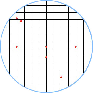
A hypothetical wafer with 7 defects and a small die. Individual die are less likely to be impacted by defects.
The big jump is naturally the opposite. You use a big die on the new process. Now instead of 1000 die sharing 100 defects, you might only have 200 die sharing 100 defects. If there’s an even distribution of defects (which isn’t how it works), the chance of a die being hit with a defect is now 50%.
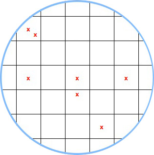
A hypothetical wafer with 7 defects and a large die.
Based on yields alone, there’s no reason you’d ever want to do a big jump. But there is good to be had from the big jump approach.
The obvious reason to do a big jump is if the things you’re going to be able to do by making huge chips (e.g. outperform the competition) will net you more revenue than if you had more of a smaller chip.
The not so obvious, but even more important reason to do a big jump is actually the reason most don’t like the big jump philosophy. Larger die are more likely to expose process problems because they will fail more often. With more opportunity to fail, you get more opportunity to see shortcomings in the process early on.
This is risky to your product, but it gives you a lot of learning that you can then use for future products based on the same process.


132 Comments
View All Comments
Dudler - Sunday, February 14, 2010 - link
Your reasoning is wrong. The 57xx is a performance segment down from the 48xx segment. By your reasoning the 5450 should be quicker than the last gen 4870X2. The 5870 should be compared to the 4870, the 5850 to 4850 and so on.Regarding price, the article sure covers it, the 40nm process was more expensive than TSMC told Amd, and the yield problems factored in too. Can't blame Amd for that can we?
And finally, don't count out that Fermi is absent to the party. Amd can charge higher prices when there is no competition. At the moment, the 5-series has a more or less monopoly in the market. Considering this, I find their prices quite fair. Don't forget nVidia launched their Gtx280 at $637....
JimmiG - Friday, February 19, 2010 - link
"Your reasoning is wrong. The 57xx is a performance segment down from the 48xx segment. "Well I compared the cards across generations based on price both at launch and how the price developed over time. The 5850 and 4850 are not in the same price segment of their respective generation. The 4850 launched at $199, the 5850 at $259 but quickly climbed to $299.
The 5770 launched at $159 and is now at $169, which is about the same as a 1GB 4870, which will perform better in DX9 and DX10. Model numbers are arbitrary and at the very best only useful for comparing cards within the same generation.
The 5k-series provide a lot of things, but certainly not value. This is the generation to skip unless you badly want to be the first to get DX11 or you're running a really old GPU.
just4U - Tuesday, February 16, 2010 - link
and they are still selling the 275,285 etc for a hefty chunk of change. I've often considered purchasing one but the price has never been right and mail in rebates are a "PASS" or "NO THANKS" for many of us rather then a incentive.I haven't seen the mail-ins for AMD products much I hope their reading this and shy away from that sort of sales format. To many of us get the shaft and never recieve our rebates anyway.
BelardA - Monday, February 15, 2010 - link
Also remind people... the current GTX 285 is about $400 and usually slower than the $300 5850. So ATI is NOT riping off people with their new DX11 products. And looking at the die-size drawings, the RV870 is a bit smaller than the GT200... and we all now that FERMI is going to be another HUGE chip.The only disappointment is that the 5750 & 5770 are not faster than the 4850/70 which used to cost about $100~120 when inventory was good. Considering that the 5700 series GPUs are smaller... Hell, even the 4770 is faster than the 5670 and costs less. Hopefully this is just the cost of production.
But I think once the 5670 is down to $80~90 and the 5700s are $100~125 - they will be more popular.
coldpower27 - Monday, February 15, 2010 - link
nVidia made a conscious decision, not to fight the 5800 Series, with the GTX 200 in terms of a price war. Hence why their price remain poor value. They won't win using a large Gt200b die vs the 5800 smaller die.Another note to keep in mind is that the 5700 Series, also have the detriment of being higher in price due to ATi moving the pricing scale backup a bit with the 5800 Series.
I guess a card that draws much less power then the 4800's, and is close to the performance of those cards is a decent win, just not completely amazing.
MonkeyPaw - Sunday, February 14, 2010 - link
Actually, the 4770 series was meant to be a suitable performance replacement for the 3870. By that scheme, the 5770 should have been comperable to the 4870. I think we just hit some diminishing returns from the 128bit GDDR5 bus.nafhan - Sunday, February 14, 2010 - link
It's the shaders not the buswidth. Bandwidth is bandwidth however you accomplish it. The rv8xx shaders are slightly less powerful on one to one basis than the rv7xx shaders are.LtGoonRush - Sunday, February 14, 2010 - link
The point is that an R5770 has 128-bit GDDR5, compared to an R4870's 256-bit GDDR5. Memory clock speeds can't scale to make up the difference from cutting the memory bus in half, so overall the card is slower, even though it has higher compute performance on the GPU. The GPU just isn't getting data from the memory fast enough.Targon - Monday, February 15, 2010 - link
But you still have the issue of the 4870 being the high end from its generation, and trying to compare it to a mid-range card in the current generation. It generally takes more than one generation before the mid range of the new generation is able to beat the high end cards from a previous generation in terms of overall performance.At this point, I think the 5830 is what competes with the 4870, or is it the 4890? In either case, it will take until the 6000 or 7000 series before we see a $100 card able to beat a 4890.
coldpower27 - Monday, February 15, 2010 - link
Yeah we haven't seen ATi/nVidia achieved the current gen mainstream faster then the last gen high end. Bandwidth issues are finally becoming apparent.6600 GT > 5950 Ultra.
7600 GT > 6800 Ultra.
But the 8600 GTS, was only marginally faster then the 7600 GT and nowhere near 7900 GTX, it took the 8800 GTS 640 to beat the 7900 GTX completely, and the 800 GTS 320 beat it, in the large majority of scenarios, due to frame buffer limitation.
The 4770 slots somewhere between the 4830/4850. However, that card was way later then most of the 4000 series. Making it a decent bit faster then the 3870, which made more sense since the jump from 3870 to 4870 was huge, sometimes nearly even 2.5x could be seen nearly, given the right conditions.
4670 was the mainstream variant and it was, most of the performance of the 3800 Series, it doesn't beat it though, more like trades blows or is slower in general.