AMD's Radeon HD 5870: Bringing About the Next Generation Of GPUs
by Ryan Smith on September 23, 2009 9:00 AM EST- Posted in
- GPUs
Cypress: What’s New
With our refresher out of the way, let’s discuss what’s new in Cypress.
Starting at the SPU level, AMD has added a number of new hardware instructions to the SPUs and sped up the execution of other instruction, both in order to improve performance and to meet the requirements of various APIs. Among these changes are that some dot products have been reduced to single-cycle computation when they were previously multi-cycle affairs. DirectX 11 required operations such as bit count, insert, and extract have also been added. Furthermore denormal numbers have received some much-needed attention, and can now be handled at full speed.
Perhaps the most interesting instruction added however is an instruction for Sum of Absolute Differences (SAD). SAD is an instruction of great importance in video encoding and computer vision due to its use in motion estimation, and on the RV770 the lack of a native instruction requires emulating it in no less than 12 instructions. By adding a native SAD instruction, the time to compute a SAD has been reduced to a single clock cycle, and AMD believes that it will result in a significant (>2x) speedup in video encoding.
The clincher however is that SAD not an instruction that’s part of either DirectX 11 or OpenCL, meaning DirectX programs can’t call for it, and from the perspective of OpenCL it’s an extension. However these APIs leave the hardware open to do what it wants to, so AMD’s compiler can still use the instruction, it just has to know where to use it. By identifying the aforementioned long version of a SAD in code it’s fed, the compiler can replace that code with the native SAD, offering the native SAD speedup to any program in spite of the fact that it can’t directly call the SAD. Cool, isn’t it?
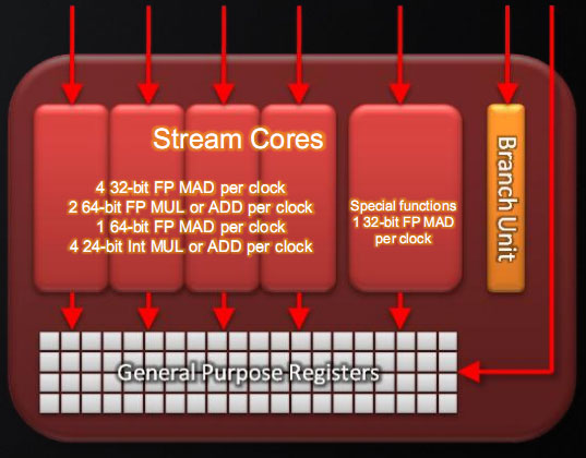
Last, here is a breakdown of what a single Cypress SP can do in a single clock cycle:
- 4 32-bit FP MAD per clock
- 2 64-bit FP MUL or ADD per clock
- 1 64-bit FP MAD per clock
- 4 24-bit Int MUL or ADD per clock
- SFU : 1 32-bit FP MAD per clock
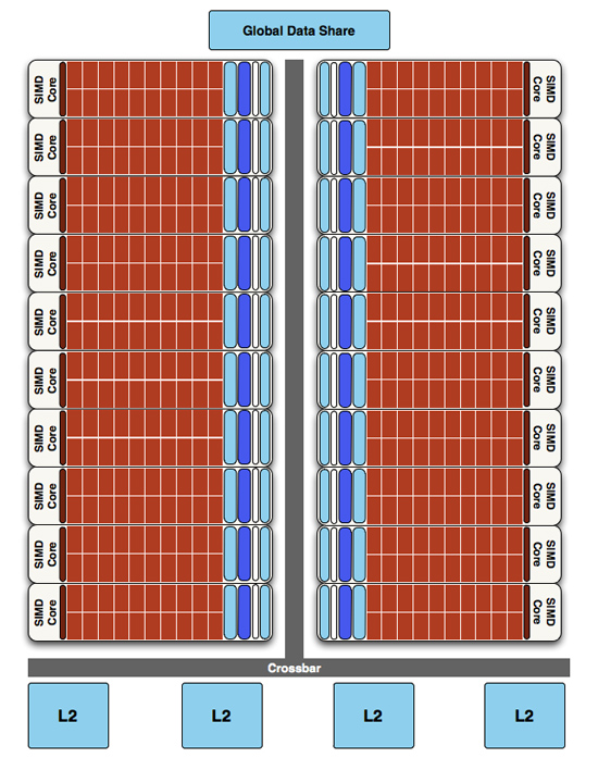
Moving up the hierarchy, the next thing we have is the SIMD. Beyond the improvements in the SPs, the L1 texture cache located here has seen an improvement in speed. It’s now capable of fetching texture data at a blistering 1TB/sec. The actual size of the L1 texture cache has stayed at 16KB. Meanwhile a separate L1 cache has been added to the SIMDs for computational work, this one measuring 8KB. Also improving the computational performance of the SIMDs is the doubling of the local data share attached to each SIMD, which is now 32KB.
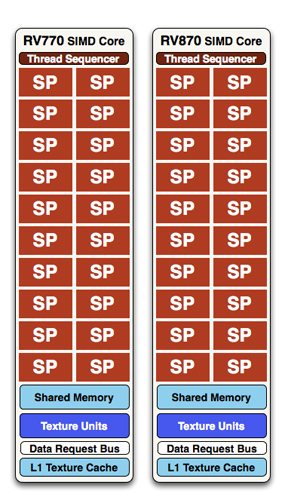
At a high level, the RV770 and Cypress SIMDs look very similar
The texture units located here have also been reworked. The first of these changes are that they can now read compressed AA color buffers, to better make use of the bandwidth they have. The second change to the texture units is to improve their interpolation speed by not doing interpolation. Interpolation has been moved to the SPs (this is part of DX11’s new Pull Model) which is much faster than having the texture unit do the job. The result is that a texture unit Cypress has a greater effective fillrate than one under RV770, and this will show up under synthetic tests in particular where the load-it and forget-it nature of the tests left RV770 interpolation bound. AMD’s specifications call for 68 billion bilinear filtered texels per second, a product of the improved texture units and the improved bandwidth to them.
Finally, if we move up another level, here is where we see the cause of the majority of Cypress’s performance advantage over RV770. AMD has doubled the number of SIMDs, moving from 10 to 20. This means twice the number of SPs and twice the number of texture units; in fact just about every statistic that has doubled between RV770 and Cypress is a result of doubling the SIMDs. It’s simple in concept, but as the SIMDs contain the most important units, it’s quite effective in boosting performance.
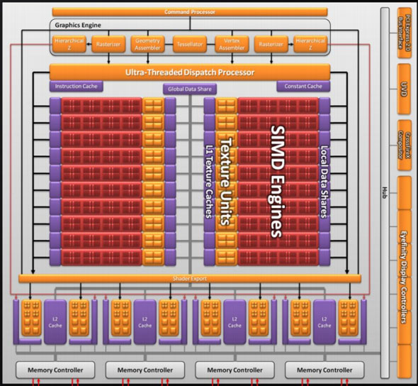
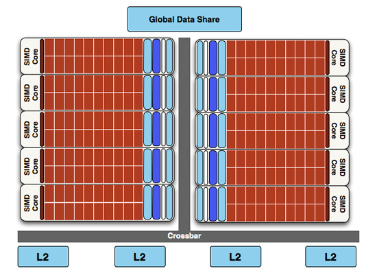
However with twice as many SIMDs, there comes a need to feed these additional SIMDs, and to do something with their products. To achieve this, the 4 L2 caches have been doubled from 64KB to 128KB. These large L2 caches can now feed data to L1 caches at 435GB/sec, up from 384GB/sec in RV770. Along with this the global data share has been quadrupled to 64KB.
RV770 vs...
Cypress
Next up, the ROPs have been doubled in order to meet the needs of processing data from all of those SIMDs. This brings Cypress to 32 ROPs. The ROPs themselves have also been slightly enhanced to improve their performance; they can now perform fast color clears, as it turns out some games were doing this hundreds of times between frames. They are also responsible for handling some aspects of AMD’s re-introduced Supersampling Anti-Aliasing mode, which we will get to later.
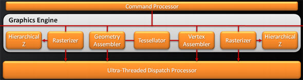
Last, but certainly not least, we have the changes to what AMD calls the “graphics engine”, primarily to bring it into compliance with DX11. RV770’s greatly underutilized tessellator has been upgraded to full DX11 compliance, giving it Hull Shader and Domain Shader capabilities, along with using a newer algorithm to reduce tessellation artifacts. A second rasterizer has also been added, ostensibly to feed the beast that is the 20 SIMDs.


327 Comments
View All Comments
mapesdhs - Saturday, September 26, 2009 - link
MODel3 writes:
> 1.Geometry/vertex performance issues ...
> 2.Geometry/vertex shading performance issues ...
Would perhaps some of the subtests in 3DMark06 be able to test this?
(not sure about Vantage, never used that yet) Though given what Jarred
said about the bandwidth and other differences, I suppose it's possible
to observe large differences in synthetic tests which are not the real
cause of a performance disparity.
The trouble with heavy GE tests is, they often end up loading the fill
rates anyway. I've run into this problem with the SGI tests I've done
over the years:
http://www.sgidepot.co.uk/sgi.html">http://www.sgidepot.co.uk/sgi.html
The larger landscape models used in the Inventor tests are a good
example. The points models worked better in this regard for testing
GE speed (stars3/star4), but I don't know to what extent modern PC
gfx is designed to handle points modelling - probably works better
on pro cards. Actually, Inventor wasn't a good choice anyway as it's
badly CPU-bound and API-heavy (I should have used Performer, gives
results 5 to 10X faster).
Anyway, point is, synthetic tests might allow one to infer that one
aspect of the gfx pipeline is a bottleneck when infact it isn't.
Ages ago I emailed NVIDIA (Ujesh, who I used to know many moons ago,
but alas he didn't reply) asking when, if ever, they would add
performance counters and other feedback monitors to their gfx
products so that applications could tell what was going on in the
gfx pipeline. SGI did this ages years ago, which allowed systems like
IR to support impressive functions such as Dynamic Video Resizing by
being able to monitor frame by frame what was going on within the gfx
engine at each stage. Try loading any 3D model into perfly, press F1
and click on 'Gfx' in the panel (Linux systems can run Performer), eg.:
http://www.sgidepot.co.uk/misc/perfly.gif">http://www.sgidepot.co.uk/misc/perfly.gif
Given how complex modern PC gfx has become, it's always been a
mystery to me why such functions haven't been included long ago.
Indeed, for all that Crysis looks amazing, I was never that keen on
it being used as a benchmark since there was no way of knowing
whether the performance hammering it created was due to a genuinely
complex environment or just an inefficient gfx engine. There's still
no way to be sure.
If we knew what was happening inside the gfx system, we could easily
work out why performance differences for different apps/games crop
up the way they do. And I would have thought that feedback monitors
within the gfx pipe would be even more useful to those using
professional applications, just as it was for coders working on SGI
hardware in years past.
Come to think of it, how do NVIDIA/ATI even design these things
without being able to monitor what's going on? Jarred, have you ever
asked either company about this?
Ian.
JarredWalton - Saturday, September 26, 2009 - link
I haven't personally, since I'm not really the GPU reviewer here. I'd assume most of their design comes from modeling what's happening, and with knowledge of their architecture they probably have utilities that help them debug stuff and figure out where stalls and bottlenecks are occurring. Or maybe they don't? I figure we don't really have this sort of detail for CPUs either, because we have tools that know the pipeline and architecture and they can model how the software performs without any hardware feedback.MODEL3 - Thursday, October 1, 2009 - link
I checked the web for synthetic geometry tests.Sadly i only found 3dMark Vantage tests.
You can't tell much from them, but they are indicative.
Check:
http://www.pcper.com/article.php?aid=783&type=...">http://www.pcper.com/article.php?aid=783&type=...
GPU Cloth: 5870 is only 1,2X faster than 4890. (vertex/geometry shading test)
GPU Particles: 5870 is only 1,2X faster than 4890. (vertex/geometry shading test)
Perlin Noise: 5870 is 2,5X faster than 4890. (Math-heavy Pixel Shader test)
Parallax Occlusion Mapping: 5870 is 2,1X faster than 4890. (Complex Pixel Shader test)
All the above 4 tests are not bandwidth limited at all.
Just for example, if you check:
http://www.pcper.com/article.php?aid=674&type=...">http://www.pcper.com/article.php?aid=674&type=...
You will see that a 750MHz 4870 512MB is 20-23% faster than a 625MHz 4850 in all the above 4 tests, so the extra bandwidth (115,2GB/s vs 64GB/s) it doesn't help at all.
But 4850 is extremely bandwidth limited in the color fillrate test (4870 is 60% faster than 4850)
Also it shouldn't be a problem of the dual rasterizer/dual SIMDs engine efficiency since synthetic Pixel Shader tests is fine (more than 2X) while the synthetic geometry shading tests is only 1,2X.
My guess is ATI didn't improve the classic geometry set-up engine and the GS because they want to promote vertex/geometry techniques based on the DX11 tesselator from now on.
Zool - Friday, September 25, 2009 - link
In Dx11 the fixed tesselation units will do much finer geometry details for much less memmory space and on chip so i think there isnt a single problem with that. Also the compute shader need minimal memory bandwith and can utilize plenty of idle shaders. The card is designed with dx11 in mind and it isnt using the wholle pipeline after all. I wouldnt make too early conclusions.(I think the perfomance will be much better after few drivers)MODEL3 - Saturday, September 26, 2009 - link
The DX11 tesselator in order to be utilized must the game engine to take advantage of it.I am not talking about the tesselator.
I am talking about the classic Geometry unit (DX9/DX10 engines) and the Geometry Shader [GS] (DX10 engines only).
I'll check to see if i can find a tech site that has synthetic bench for Geometry related perf. and i will post again tomorrow, if i can find anything.
JarredWalton - Friday, September 25, 2009 - link
It's worth noting that when you factor in clock speeds, compared to the 5870 the 4870X2 offers 88% of the core performance and 50% more bandwidth. Some algorithms/games require more bandwidth and others need more core performance, but it's usually a combination of the two. The X2 also has CrossFire inefficiencies to deal with.More interesting perhaps is that the GTX 295 offers (by my estimates, which admittedly are off in some areas) roughly 10% more GPU shader performance, about 18.5% more fill rate, and 46% more bandwidth than the HD 5870. The fact that the HD 4870 is still competitive is a good sign that ATI is getting good use of their 5 SPs per Stream Processor design, and that they are not memory bandwidth limited -- at least not entirely.
SiliconDoc - Wednesday, September 30, 2009 - link
The 4870x2 has somewhere around "double the data paths" in and out of it's 2 cpu's. So what you have with the 5870 putting as some have characterized " 2x 770 cores melded into one " is DOUBLE THE BOTTLENECK in and out of the core.They tried to compensate with ddr5 1200/4800 - but the fact remains, they only get so much with that "NOT ENOUGH DATA PATHS/PINS in and out of that gpu core."
cactusdog - Friday, September 25, 2009 - link
Omg these cards look great. Lol Silicon Doc is so gutted and furious he is making hmself look like a dam fool again only this time he should be on suicide watch...Nvidia cards are now obsolete..LOL.mapesdhs - Friday, September 25, 2009 - link
Hehe, indeed. Have you ever seen a scifi series called, "They Came
From Somewhere Else?" S.D.'s getting so worked up, reminds me of
the scene where the guy's head explodes. :D
Hmm, that's an alternative approach I suppose in place of post
moderation. Just get someone so worked up about something they'll
have an aneurism and pop their clogs... in which case, I'll hand
it back to Jarred. *grin*
Ian.
SiliconDoc - Friday, September 25, 2009 - link
That is quite all right, you fellas make sure to read it all, I am more than happy that the truth is sinking into your gourds, you won't be able to shake it.I am very happy about it.