AMD's Radeon HD 5870: Bringing About the Next Generation Of GPUs
by Ryan Smith on September 23, 2009 9:00 AM EST- Posted in
- GPUs
Cypress: What’s New
With our refresher out of the way, let’s discuss what’s new in Cypress.
Starting at the SPU level, AMD has added a number of new hardware instructions to the SPUs and sped up the execution of other instruction, both in order to improve performance and to meet the requirements of various APIs. Among these changes are that some dot products have been reduced to single-cycle computation when they were previously multi-cycle affairs. DirectX 11 required operations such as bit count, insert, and extract have also been added. Furthermore denormal numbers have received some much-needed attention, and can now be handled at full speed.
Perhaps the most interesting instruction added however is an instruction for Sum of Absolute Differences (SAD). SAD is an instruction of great importance in video encoding and computer vision due to its use in motion estimation, and on the RV770 the lack of a native instruction requires emulating it in no less than 12 instructions. By adding a native SAD instruction, the time to compute a SAD has been reduced to a single clock cycle, and AMD believes that it will result in a significant (>2x) speedup in video encoding.
The clincher however is that SAD not an instruction that’s part of either DirectX 11 or OpenCL, meaning DirectX programs can’t call for it, and from the perspective of OpenCL it’s an extension. However these APIs leave the hardware open to do what it wants to, so AMD’s compiler can still use the instruction, it just has to know where to use it. By identifying the aforementioned long version of a SAD in code it’s fed, the compiler can replace that code with the native SAD, offering the native SAD speedup to any program in spite of the fact that it can’t directly call the SAD. Cool, isn’t it?
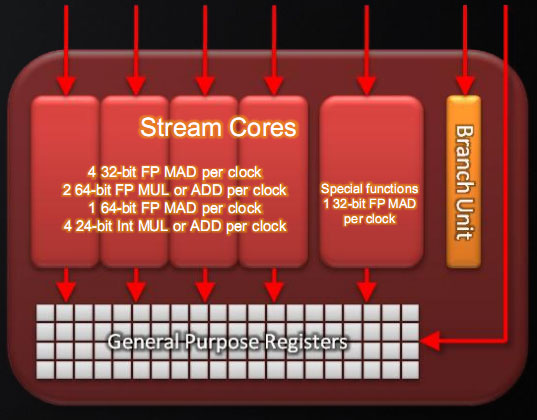
Last, here is a breakdown of what a single Cypress SP can do in a single clock cycle:
- 4 32-bit FP MAD per clock
- 2 64-bit FP MUL or ADD per clock
- 1 64-bit FP MAD per clock
- 4 24-bit Int MUL or ADD per clock
- SFU : 1 32-bit FP MAD per clock
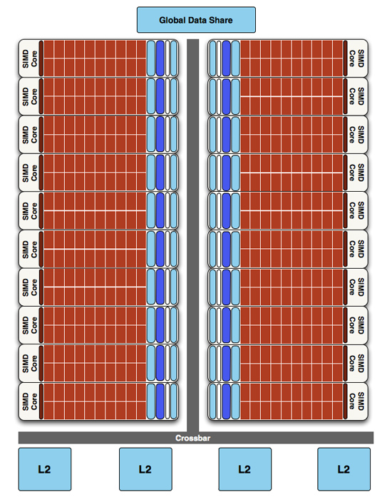
Moving up the hierarchy, the next thing we have is the SIMD. Beyond the improvements in the SPs, the L1 texture cache located here has seen an improvement in speed. It’s now capable of fetching texture data at a blistering 1TB/sec. The actual size of the L1 texture cache has stayed at 16KB. Meanwhile a separate L1 cache has been added to the SIMDs for computational work, this one measuring 8KB. Also improving the computational performance of the SIMDs is the doubling of the local data share attached to each SIMD, which is now 32KB.
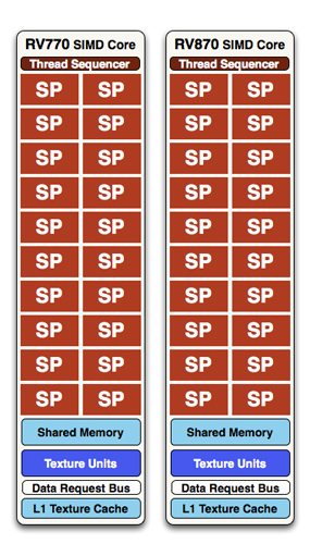
At a high level, the RV770 and Cypress SIMDs look very similar
The texture units located here have also been reworked. The first of these changes are that they can now read compressed AA color buffers, to better make use of the bandwidth they have. The second change to the texture units is to improve their interpolation speed by not doing interpolation. Interpolation has been moved to the SPs (this is part of DX11’s new Pull Model) which is much faster than having the texture unit do the job. The result is that a texture unit Cypress has a greater effective fillrate than one under RV770, and this will show up under synthetic tests in particular where the load-it and forget-it nature of the tests left RV770 interpolation bound. AMD’s specifications call for 68 billion bilinear filtered texels per second, a product of the improved texture units and the improved bandwidth to them.
Finally, if we move up another level, here is where we see the cause of the majority of Cypress’s performance advantage over RV770. AMD has doubled the number of SIMDs, moving from 10 to 20. This means twice the number of SPs and twice the number of texture units; in fact just about every statistic that has doubled between RV770 and Cypress is a result of doubling the SIMDs. It’s simple in concept, but as the SIMDs contain the most important units, it’s quite effective in boosting performance.
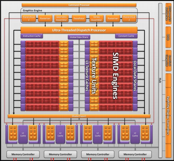
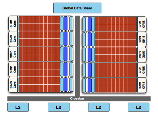
However with twice as many SIMDs, there comes a need to feed these additional SIMDs, and to do something with their products. To achieve this, the 4 L2 caches have been doubled from 64KB to 128KB. These large L2 caches can now feed data to L1 caches at 435GB/sec, up from 384GB/sec in RV770. Along with this the global data share has been quadrupled to 64KB.
RV770 vs...
Cypress
Next up, the ROPs have been doubled in order to meet the needs of processing data from all of those SIMDs. This brings Cypress to 32 ROPs. The ROPs themselves have also been slightly enhanced to improve their performance; they can now perform fast color clears, as it turns out some games were doing this hundreds of times between frames. They are also responsible for handling some aspects of AMD’s re-introduced Supersampling Anti-Aliasing mode, which we will get to later.
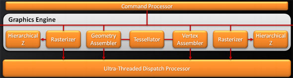
Last, but certainly not least, we have the changes to what AMD calls the “graphics engine”, primarily to bring it into compliance with DX11. RV770’s greatly underutilized tessellator has been upgraded to full DX11 compliance, giving it Hull Shader and Domain Shader capabilities, along with using a newer algorithm to reduce tessellation artifacts. A second rasterizer has also been added, ostensibly to feed the beast that is the 20 SIMDs.


327 Comments
View All Comments
Zool - Sunday, September 27, 2009 - link
The speed of the on chip cache just shows that the external memory bandwith in curent gpus is only to get the data to gpu or recieve the final data from gpu. The raw processing hapenns on chip with those 10 times faster sram cache or else the raw teraflops would vanish.JarredWalton - Sunday, September 27, 2009 - link
If SD had any reading comprehension or understanding of tech, he would realize that what I am saying is:1) Memory bandwidth didn't double - it went up by just 23%
2) Look at the results and performance increased by far more than 23%
3) Ergo, the 4890 is not bandwidth limited in most cases, and there was no need to double the bandwidth.
Would more bandwidth help performance? Almost certainly, as the 5870 is such a high performance part that unlike the 4890 it could use more. Similarly, the 4870X2 has 50% more bandwidth than the 5870, but it's never 50% faster in our tests, so again it's obviously not bandwidth limited.
Was it that hard to understand? Nope, unless you are trying to pretend I put an ATI bias on everything I say. You're trying to start arguments again where there was none.
SiliconDoc - Sunday, September 27, 2009 - link
The 4800 data rate ram is faster vs former 3600 - hence bus width is running FASTER - so your simple conclusions are wrong.When we overlcock the 5870's ram, we get framerate increase - it increases the bandwidth, and up go the numbers.
---
Not like there isn't an argument, because you don't understand tech.
JarredWalton - Sunday, September 27, 2009 - link
The bus is indeed faster -- 4800 effective vs. 3900 on the 4890 or 3600 on the 4870. What's "wrong about my simple conclusions"? You're not wrong, but you're not 100% right if you suggest bandwidth is the only bottleneck.Naturally, as most games are at least partially bandwidth limited, if you overclock 10% you increase performance. The question is, does it increase linearly by 10%? Rarely, just as if you overclock the core 10% you usually don't get 10% boost. If you do get a 1-for-1 increase with overclocking, it indicates you are solely bottlenecked by that aspect of performance.
So my conclusions still stand: the 5870 is more bandwidth limited than 4890, but it is not completely bandwidth limited. Improving the caches will also help the GPU deal with less bandwidth, just as it does on CPUs. As fast as Bloomfield may be with triple-channel DDR3-1066 (25.6GB/s), the CPU can process far more data than RAM could hope to provide. Would a wider/faster bus help the 5870? Yup. Would it be a win-win scenario in terms of cost vs. performance? Apparently ATI didn't think so, and given how quickly sales numbers taper off above $300 for GPUs, I'm inclined to agree.
I'd also wager we're a lot more CPU limited on 5870 than many other GPUs, particularly with CrossFire setups. I wouldn't even look at 5870 CrossFire unless you're running a high-end/overclocked Core i7 or Phenom II (i.e. over ~3.4GHz).
And FWIW: Does any of this mean NVIDIA can't go a different route? Nope. GT300 can use 512-bit interfaces with GDDR5, and they can be faster than 5870. They'll probably cost more if that's the case, but then it's still up to the consumers to decide how much they're willing to spend.
silverblue - Saturday, September 26, 2009 - link
I suppose if we end up seeing a 512-bit card then it'll make for a very interesting comparison with the 5870. With equal clocks during testing, we'd have a far better idea, though I'd expect to see far more RAM on a 512-bit card which may serve to skew the figures and muddy the waters, so to speak.Voo - Friday, September 25, 2009 - link
Hey Jarred I know that's neither the right place nor the right person to ask, but do we get some kind of "Ignore this person" button with the site revamp Anand talked about some months ago?I think I'd prefer this feature about almost everything - even an edit button ;)
JarredWalton - Friday, September 25, 2009 - link
I'll ask and find out. I know that the comments are supposed to receive a nice overhaul, but more than that...? Of course, if you ignore his posts on this (and the responses), you'd only have about five comments! ;-)Voo - Saturday, September 26, 2009 - link
Great!Yep it'd be rather short, but I'd rather have 10 interesting comments than 1000 COMMENTS WRITTEN IN CAPS!!11 with dubious content ;)
SiliconDoc - Wednesday, September 30, 2009 - link
I put it in caps so you could easily avoid them, I was thinking of you and your "problems".I guess since you "knew this wasn't the right time or place" but went ahead anyway, you've got "lot's of problems".
Let me know when you have posted an "interesting comment" with no "dubios nature" to it.
I suspect I'll be waiting years.
MODEL3 - Friday, September 25, 2009 - link
Hi Ryan,Nice new info in your review.
The day you posted your review, i wrote in the forums that according to my perception there are other reasons except bandwidth limitations and driver maturity, that the 850MHz 5870 hasn't doubled its performance in relation with a 850MHz 4890.
Usually when a GPU has 2X the specs of another GPU the performance gain is 2X (of cource i am not talking about games with engines that are CPU limited or engines that seems to scale badly or are poor coded for example)
There are many examples in the past that we had 2X performance gain with 2X the specs. (not in all the games, but in many games)
From the tests that i saw in your review and from my understanding of the AMD slides, i think there are 2 more reasons that 5870 performs like that.
The day of your review i wrote to the forums the additional reasons that i think the 5870 performs like that, but nobody replied me.
I wrote that probably 5870 has:
1.Geometry/vertex performance issues (in the sense that it cannot generate 2X geometry in relation with 4890) (my main assumption)
or/and
2.Geometry/vertex shading performance issues (in the sense that the geometry shader [GS] cannot shade vertex with 2X speed in relation with 4890)(another possible assumption)
I guess there are synthetic benchmarks that have tests like that (pure geometry speed, and pure geometry/vertex shader speed, in addition with the classic pixel shader speed tests) so someone can see if my assumption is true.
If you have the time and you think that this is possible and you feel like it is worth your time, can you check my hypothesis please?
Thanks very much,
MODel3