AMD's Radeon HD 5870: Bringing About the Next Generation Of GPUs
by Ryan Smith on September 23, 2009 9:00 AM EST- Posted in
- GPUs
A Quick Refresher on the RV770
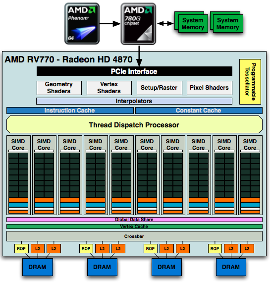
As Cypress is a direct evolution of the RV770 design, before we talk about what’s new with Cypress we are going to go over a quick rehash of RV770’s internal workings. As it’s necessary to understand how RV770 was built to understand what Cypress changes, if you’re completely unfamiliar with RV770, please take a look at our expanded discussion of RV770 from last year. For the rest of you, let’s get started.
At the center of the RV770 is the Stream Processing Unit (SPU), a single arithmetic logic unit. The RV770 has 800 of these, and they are packaged together in groups of 5 and are what we call a Streaming Processor (SP). A SP contains a register file, a branch predictor, and the aforementioned 5 SPUs, with the 5th SPU being a more complex unit capable of transcendental functions along with the base functions of an ALU. The SP is the smallest unit that can do individual work; every SPU in an SP must execute the same instruction.
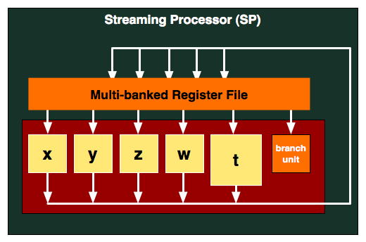
For every 16 SPs, AMD groups them together with texture units, L1 cache, shared memory, and controlling logic. This combined block is what AMD calls a SIMD, and RV770 has 10 of them. These 10 SIMDs form the core computational power of the RV770, and in the chip work with various specialized units such as ROPs, rasterizers, L2 cache, and tesselators to form a complete chip.
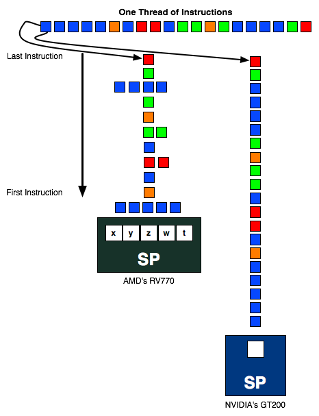
To utilize the computational power of the hardware, instruction threads are issued to the SPs. These threads are grouped into wavefronts, where there are 64 threads per wavefront. To maximize the utilization of the GPU, threads need to be organized so that they can feed all 5 SPUs in a SP an instruction every clock cycle. Doing this requires extracting instruction level parallelism (ILP) out of programs being passed to the GPU, which is difficult task of AMD’s compiler.
If SPUs go unused, then the performance of the chip suffers due to underutilization. This design gives AMD a great deal of theoretical computational power, but it is always a challenge to fully exploit it.


327 Comments
View All Comments
erple2 - Wednesday, September 23, 2009 - link
I think that you're missing the point. AMD appeared to want the part to be small enough to maximize the number of gpu's generated per wafer. They had their own internal idea of how to get a good yield from the 40nm wafers.It appears to be similar to their line of thinking with the 4870 launch (see http://www.anandtech.com/video/showdoc.aspx?i=3469">http://www.anandtech.com/video/showdoc.aspx?i=3469 for more information) - they didn't feel like they needed to get the biggest, fastest, most power hungry part to compete well. It turns out that with the 5870, they have that, at least until we see what Nvidia comes out with the G300.
It turns out that performance really isn't all people care about - otherwise nobody would run anything other than dual GTX285's in SLI. People care about performance __at a particular price point__. ATI is trying to grab that particular sweet spot - be able to take the performance crown for a particular price range. They would probably be able to make a gargantuan low-yield, high power monster that would decimate everything currently available (crossfire/SLI or single), but that chip would be massively expensive to produce, and surprisingly, be a poor Return on Investment.
So the comment that Cypress is "too big" I think really is apropos. I think that AMD would have been able to launch the 5870 at the $299 price point of the 4870 only if the die had been significantly smaller (around the same size as the 4870). THAT would have been an amazing bang-for-buck card, I believe.
Doormat - Wednesday, September 23, 2009 - link
[Big Chart] and suchfaxon - Wednesday, September 23, 2009 - link
page 15 is missing its charts guys! look at it, how did that happen lmaoGary Key - Wednesday, September 23, 2009 - link
Ryan is updating the page now. He should be finished up shortly. We had a lot of images that needed to be displayed in a different manner at the last minute.Totally - Wednesday, September 23, 2009 - link
the images are missingdguy6789 - Wednesday, September 23, 2009 - link
You very clearly fail to mention that the cheapest GTX295 one can buy is nearly $100 more expensive than the HD 5870.Ryan Smith - Wednesday, September 23, 2009 - link
In my own defense, when I wrote that paragraph Newegg's cheapest brand-new GTX 295 was only $409. They've been playing price games...SiliconDoc - Friday, September 25, 2009 - link
That "price game" is because the 5870 is rather DISAPPOINTING when compared to the GTX295.I guess that means ATI "blew the competition" this time, huh, and NVidia is going to get more money for their better GTX295.
LOL
That's a *scowl* "new egg price game" for red fans.
Thanks ATI for making NVidia more money !
strikeback03 - Wednesday, September 23, 2009 - link
lol, did they drop the price while they had 5870s in stock, then raise it again once they were gone?SiliconDoc - Wednesday, September 23, 2009 - link
Oh, so sorry, 1:46pm, NO 5870's available at the egg...I guess they sold 1 powercolor and one asus...
http://www.newegg.com/Product/ProductList.aspx?Sub...">http://www.newegg.com/Product/ProductLi...1&na...
---
Come on anandtech workers, you can say it "PAPER LUANCH !"