AMD's Radeon HD 5870: Bringing About the Next Generation Of GPUs
by Ryan Smith on September 23, 2009 9:00 AM EST- Posted in
- GPUs
Lower Idle Power & Better Overcurrent Protection
One aspect AMD was specifically looking to improve in Cypress over RV770 was idle power usage. The load power usage for RV770 was fine at 160W for the HD4870, but that power usage wasn’t dropping by a great deal when idle – it fell by less than half to 90W. Later BIOS revisions managed to knock a few more watts off of this, but it wasn’t a significant change, and even later designs like RV790 still had limits to their idling abilities by only being able to go down to 60W at idle.
As a consequence, AMD went about designing the Cypress with a much, much lower target in mind. Their goal was to get idle power down to 30W, 1/3rd that of RV770. What they got was even better: they came in past that target by 10%, hitting a final idle power of 27W. As a result the Cypress can idle at 30% of the power as RV770, or as compared to Cypress’s load power of 188W, some 14% of its load power.
Accomplishing this kind of dramatic reduction in idle power usage required several changes. Key among them has been the installation of additional power regulating circuitry on the board, and additional die space on Cypress assigned to power regulation. Notably, all of these changes were accomplished without the use of power-gating to shut down unused portions of the chip, something that’s common on CPUs. Instead all of these changes have been achieved through more exhaustive clock-gating (that is, reducing power consumption by reducing clock speeds), something GPUs have been doing for some time now.
The use of clock-gating is quickly evident when we discuss the idle/2D clock speeds of the 5870, which is 150mhz for the core, and 300mhz for the memory . The idle clock speeds here are significantly lower than the 4870 (550/900), which in the case of the core is the source of its power savings as compared to the 4870. As tweakers who have attempted to manually reduce the idle clocks on RV770 based cards for further power savings have noticed, RV770 actually loses stability in most situations if its core clock drops too low. With the Cypress this has been rectified, enabling it to hit these lower core speeds.
Even bigger however are the enhancements to Cypress’s memory controller, which allow it to utilize a number of power-saving tricks with GDDR5 RAM, along with other features that we’ll get to in a bit. With RV770’s memory controller, it was not capable of taking advantage of very many of GDDR5’s advanced features besides the higher bandwidth abilities. Lacking this full bag of tricks, RV770 and its derivatives were unable to reduce the memory clock speed, which is why the 4870 and other products had such high memory clock speeds even at idle. In turn this limited the reduction in power consumption attained by idling GDDR5 modules.
With Cypress AMD has implemented nearly the entire suite of GDDR5’s power saving features, allowing them to reduce the power usage of the memory controller and the GDDR5 modules themselves. As with the improvements to the core clock, key among the improvement in memory power usage is the ability to go to much lower memory clock speeds, using fast GDDR5 link re-training to quickly switch the memory clock speed and voltage without inducing glitches. AMD is also now using GDDR5’s low power strobe mode, which in turn allows the memory controller to save power by turning off the clock data recovery mechanism. When discussing the matter with AMD, they compared these changes to putting the memory modules and memory controller into a GDDR3-like mode, which is a fair description of how GDDR5 behaves when its high-speed features are not enabled.
Finally, AMD was able to find yet more power savings for Crossfire configurations, and as a result the slave card(s) in a Crossfire configuration can use even less power. The value given to us for an idling slave card is 20W, which is a product of the fact that the slave cards go completely unused when the system is idling. In this state slave cards are still capable of instantaneously ramping up for full-load use, although conceivably AMD could go even lower still by powering down the slave cards entirely at a cost of this ability.
On the opposite side of the ability to achieve such low idle power usage is the need to manage load power usage, which was also overhauled for the Cypress. As a reminder, TDP is not an absolute maximum, rather it’s a maximum based on what’s believed to be the highest reasonable load the card will ever experience. As a result it’s possible in extreme circumstances for the card to need power beyond what its TDP is rated for, which is a problem.
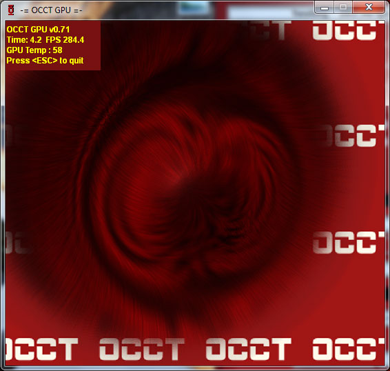
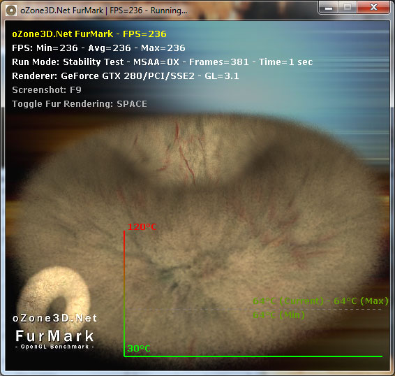
That problem reared its head a lot for the RV770 in particular, with the rise in popularity of stress testing programs like FurMark and OCCT. Although stress testers on the CPU side are nothing new, FurMark and OCCT heralded a new generation of GPU stress testers that were extremely effective in generating a maximum load. Unfortunately for RV770, the maximum possible load and the TDP are pretty far apart, which becomes a problem since the VRMs used in a card only need to be spec’d to meet the TDP of a card plus some safety room. They don’t need to be able to meet whatever the true maximum load of a card can be, as it should never happen.
Why is this? AMD believes that the instruction streams generated by OCCT and FurMark are entirely unrealistic. They try to hit everything at once, and this is something that they don’t believe a game or even a GPGPU application would ever do. For this reason these programs are held in low regard by AMD, and in our discussions with them they referred to them as “power viruses”, a term that’s normally associated with malware. We don’t agree with the terminology, but in our testing we can’t disagree with AMD about the realism of their load – we can’t find anything that generates the same kind of loads as OCCT and FurMark.
Regardless of what AMD wants to call these stress testers, there was a real problem when they were run on RV770. The overcurrent situation they created was too much for the VRMs on many cards, and as a failsafe these cards would shut down to protect the VRMs. At a user level shutting down like this isn’t a very helpful failsafe mode. At a hardware level shutting down like this isn’t enough to protect the VRMs in all situations. Ultimately these programs were capable of permanently damaging RV770 cards, and AMD needed to do something about it. For RV770 they could use the drivers to throttle these programs; until Catalyst 9.8 they detected the program by name, and since 9.8 they detect the ratio of texture to ALU instructions (Ed: We’re told NVIDIA throttles similarly, but we don’t have a good control for testing this statement). This keeps RV770 safe, but it wasn’t good enough. It’s a hardware problem, the solution needs to be in hardware, particularly if anyone really did write a power virus in the future that the drivers couldn’t stop, in an attempt to break cards on a wide scale.
This brings us to Cypress. For Cypress, AMD has implemented a hardware solution to the VRM problem, by dedicating a very small portion of Cypress’s die to a monitoring chip. In this case the job of the monitor is to continually monitor the VRMs for dangerous conditions. Should the VRMs end up in a critical state, the monitor will immediately throttle back the card by one PowerPlay level. The card will continue operating at this level until the VRMs are back to safe levels, at which point the monitor will allow the card to go back to the requested performance level. In the case of a stressful program, this can continue to go back and forth as the VRMs permit.
By implementing this at the hardware level, Cypress cards are fully protected against all possible overcurrent situations, so that it’s not possible for any program (OCCT, FurMark, or otherwise) to damage the hardware by generating too high of a load. This also means that the protections at the driver level are not needed, and we’ve confirmed with AMD that the 5870 is allowed to run to the point where it maxes out or where overcurrent protection kicks in.
On that note, because card manufacturers can use different VRMs, it’s very likely that we’re going to see some separation in performance on FurMark and OCCT based on the quality of the VRMs. The cheapest cards with the cheapest VRMs will need to throttle the most, while luxury cards with better VRMs would need to throttle little, if at all. This should make little difference in stock performance on real games and applications (since as we covered earlier, we can’t find anything that pushes a card to excess) but it will likely make itself apparent in overclocking. Overclocked cards - particularly those with voltage modifications – may hit throttle situations in normal applications, which means the VRMs will make a difference here. It also means that overclockers need to keep an eye on clock speeds, as the card shutting down is no longer a tell-tale sign that you’re pushing it too hard.
Finally, while we’re discussing the monitoring chip, we may as well talk about the rest of its features. Along with monitoring the GPU, it also is a PWM controller. This means that the PWM controller is no longer a separate part that card builders add themselves, and as such we won’t be seeing any cards using a 2pin fixed speed fan to save money on the PWM controller. All Cypress cards (and presumably, all derivatives) will have the ability to use a 4pin fan built-in.


327 Comments
View All Comments
BoFox - Friday, November 6, 2009 - link
Yep, that's turning up LOD to -1 or -2 depending on which game. It was done in Crysis, and with LOD at -2, it looked sharp with SSAA.The Wasrad - Wednesday, September 23, 2009 - link
Why are you using 4 gigs of ram with a 920?Do you understand how DDR3 memory works?
Ryan Smith - Wednesday, September 23, 2009 - link
Error when writing the chart. It has been corrected.Sc4freak - Wednesday, September 23, 2009 - link
Do you? The fact that the i7 920 works best in a triple-channel configuration has nothing to do with the fact that it uses DDR3.chizow - Wednesday, September 23, 2009 - link
Agreed and to add to that, the fact the third channel means very little when it comes to actual gaming performance makes it even less signficant. As compared to Lynnfield clock for clock, which is only dual channel:http://www.anandtech.com/cpuchipsets/showdoc.aspx?...">http://www.anandtech.com/cpuchipsets/showdoc.aspx?...
Von Matrices - Wednesday, September 23, 2009 - link
Could someone enlighten me as to why the 4870 X2 could be faster than the 5870 in some situations? It was noted it the article but never really explained. They have the same number of SP's, and one would expect crossfire scaling to be detrimental to the 4870 X2"s performance. Would this be indicative of the 5870 being starved for memory bandwidth in these situations or something else?Dobs - Wednesday, September 23, 2009 - link
4870x2 has 2Gb of DDR55870 only has 1 until the 2Gb edition comes out :)
nafhan - Wednesday, September 23, 2009 - link
Doesn't using dual GPU's effectively halve the onboard memory, as significant portions of the textures, etc. need to be duplicated? So, the 4870x2 has a memory disadvantage by requiring 2x memory to accomplish the same thing.chizow - Wednesday, September 23, 2009 - link
Right, with an X2 each GPU has a copy of the same frame buffer, so the total memory onboard is effectively halved. A 2GB frame buffer with 2 GPU is two of the same 1GB frame buffer mirrored on each.With the 5870 essentially being 2xRV790 on one chip, in order to accomplish the same frame rates on the same sized 1GB frame buffer, you would expect to need additional bandwidth to facilitate the transfers to and from the frame buffer and GPU.
chizow - Wednesday, September 23, 2009 - link
Ya he mentions bandwidth being a potential issue preventing the 5870 from mirroring the 4870X2's results.It could also be that the 5870's scheduler/dispatch processor aren't as efficient at extracting performance as driver forced AFR. Seems pretty incredible, seeing as physically doubling GPU transistors on a single die has always been traditionally better than multi-GPU scaling.
Similarly, it could be a CPU limitation where CF/SLI benefit more from multi-threaded driver performance, whereas a single GPU would be limited to a single fast thread or core's performance. We saw this a bit as well last year with the GT200s compared to G92s in SLI.