The SSD Anthology: Understanding SSDs and New Drives from OCZ
by Anand Lal Shimpi on March 18, 2009 12:00 AM EST- Posted in
- Storage
The Anatomy of an SSD
Let’s meet Mr. N-channel MOSFET again:
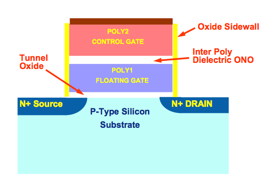
Say Hello
This is the building block of NAND-flash; one transistor is required per cell. A single NAND-flash cell can either store one or two bits of data. If it stores one, then it’s called a Single Level Cell (SLC) flash and if it stores two then it’s a Multi Level Cell (MLC) flash. Both are physically made the same way; in fact there’s nothing that separates MLC from SLC flash, it’s just a matter of how the data is stored in and read from the cell.
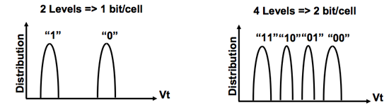
SLC flash (left) vs. MLC flash (right)
Flash is read from and written to in a guess-and-test fashion. You apply a voltage to the cell and check to see how it responds. You keep increasing the voltage until you get a result.
| SLC NAND flash | MLC NAND flash | |
| Random Read | 25 µs | 50 µs |
| Erase | 2ms per block | 2ms per block |
| Programming | 250 µs | 900 µs |
With four voltage levels to check, MLC flash takes around 3x longer to write to as SLC. On the flip side you get twice the capacity at the same cost. Because of this distinction, and the fact that even MLC flash is more than fast enough for a SSD, you’ll only see MLC used for desktop SSDs while SLC is used for enterprise level server SSDs.
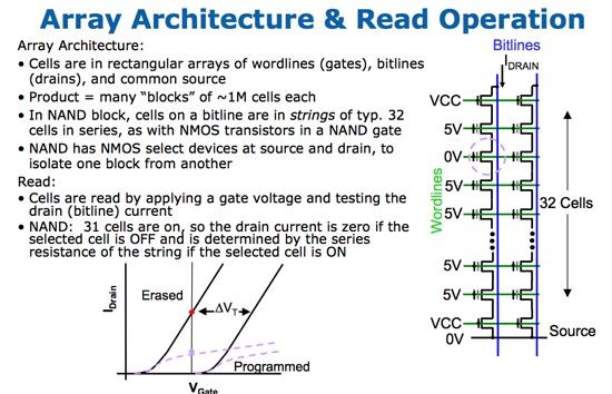
Cells are strung together in arrays as depicted in the image to the right
So a single cell stores either one or two bits of data, but where do we go from there? Groups of cells are organized into pages, the smallest structure that’s readable/writable in a SSD. Today 4KB pages are standard on SSDs.
Pages are grouped together into blocks; today it’s common to have 128 pages in a block (512KB in a block). A block is the smallest structure that can be erased in a NAND-flash device. So while you can read from and write to a page, you can only erase a block (128 pages at a time). This is where many of the SSD’s problems stem from, I’ll repeat this again later because it’s one of the most important parts of understanding SSDs.
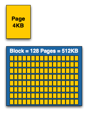
Arrays of cells are grouped into a page, arrays of pages are grouped into blocks
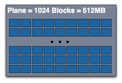
Blocks are then grouped into planes, and you’ll find multiple planes on a single NAND-flash die.
The combining doesn’t stop there; you can usually find either one, two or four die per package. While you’ll see a single NAND-flash IC, there may actually be two or four die in that package. You can also stack multiple ICs on top of each other to minimize board real estate usage.


250 Comments
View All Comments
blackburried - Wednesday, March 25, 2009 - link
It's referred to as "discard" in the kernel functions.It works very well w/ SSD's that support TRIM, like fusion-io's drives.
Iger - Wednesday, March 25, 2009 - link
This is the best review I've read in a very long time.Thank you very much!
BailoutBenny - Tuesday, March 24, 2009 - link
Great in depth article on flash based SSDs. I'm waiting for PRAM though.orclordrh - Tuesday, March 24, 2009 - link
Very illuminating article, very well written and researched. It made me glad that I didn't pull the trigger on an SSD for my I7 machine and regret not buying OCZ memory! I'm interested in adding an SSD as the scratch disk for Photoshop CS4 to use. I don't really launch applications very often, say once a week on the weekly reboot and keep 6-8 apps open at all times. I have 12GB of memory for that. The benchmarks were very interesting, but what sort of activity does Photoshop scratch usage create? Large files or random writes? What type of SSD would be most cost effective here?An SSD does sound better than a SSD!
semo - Wednesday, March 25, 2009 - link
wait for ddr3 to enter the mainstream and buy loads of memory.use a ramdisk for your adobe scratch area. much faster than ssd and no wear to worry about (not that you would worry that much with modern ssds anyway).
http://www.ghacks.net/2007/12/14/use-a-ramdisk-to-...">http://www.ghacks.net/2007/12/14/use-a-ramdisk-to-...
there is also a paid for and more feature rich ramdisk out there. can't remember the name
strikeback03 - Wednesday, March 25, 2009 - link
I'll have to check when I get home, but I believe the recommended size for the scratch disk is upwards of 10GB. So would need a motherboard that supports a LOT of RAM to give enough to main memory plus a scratch disk.strikeback03 - Wednesday, March 25, 2009 - link
I was wondering the same thing. I'd guess it would be a lot of writing/erasing, so an SSD might not be the best from a longevity standpoint, but if your system is hitting the scratch disk often then the speed might make it worthwhile.mikepers - Tuesday, March 24, 2009 - link
Anand,I wanted to compliment you on what I think was an excellent article. This is the type of thing I really have always liked from Anandtech. The detailed background, the technical reasons for the issues and then a thorough review of the current state of things.
I just finished upgrading my desktop. The only remaining item I wanted to replace was the hard disk. I had been thinking about getting a Velociraptor but instead I just ordered a 60GB Vertex from Newegg.
Thanks again for all the work.
Mike P.
ameatypie - Monday, March 23, 2009 - link
That sure was a lot to take in! Fantastic article though, it has really opened my eyes to the possibilities that Solid State Drives provide. Probably wont be buying one in the immediate future given the so-called depression and such things, but i will certainly keep up with SSD progress.Thanks again for your fantastic articles - im sure im not the only one who really appreciates them :)
coopchennick - Monday, March 23, 2009 - link
Hey Anand, I just finished reading through this whole article and I'm very impressed with the thoroughness and how informative it was.You just acquired a new regular reader.