Intel's 32nm Update: The Follow-on to Core i7 and More
by Anand Lal Shimpi on February 11, 2009 12:00 AM EST- Posted in
- CPUs
The Manufacturing Roadmap
The tick-tock cadence may have come about at the microprocessor level, but its roots have always been in manufacturing. As long as I’ve been running AnandTech, Intel has introduced a new manufacturing process every two years. In fact, since 1989 Intel has kept up this two year cycle.
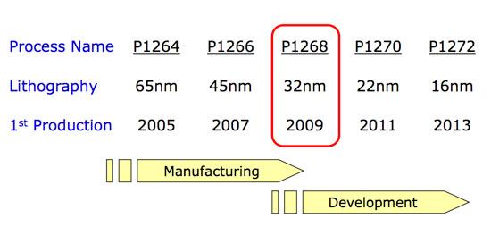
We saw the first 45nm CPUs with the Penryn core back in late 2007. Penryn, released at the very high end, spent most of 2008 making its way mainstream. Now you can buy a 45nm Penryn CPU for less than $100.
The next process technology, which Intel refers to internally as P1268, shrinks transistor feature size down to 32nm. The table above shows you that first production will be in 2009 and, after a brief pause to check your calendars, that means this year. More specifically, Q4 of this year.
I’ll get to the products in a moment, but first let’s talk about the manufacturing process itself.
Here we have our basic CMOS transistor:
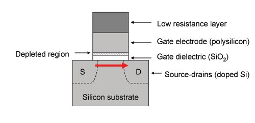
Current flows from source to drain when the transistor is on, and it isn’t supposed to flow when it’s off. Now as you shrink the transistor, all of its parts shrink. At 65nm Intel found that it couldn’t shrink the gate dielectric any more without leaking too much current through the gate itself. Back then the gate dielectric was 1.2nm thick (about the thickness of 5 atoms), but at 45nm Intel’s switched from a SiO2 gate dielectric to a high-k one using Hafnium. That’s where the high-k comes from.
The gate electrode also got replaced at 45nm with a metal to help increase drive current (more current flows when you want it to). That’s where the metal gate comes from.
The combination of the two changes to the basic transistor gave us Intel’s high-k + metal gate transistors at 45nm, and at 32nm we have the second generation of those improvements.
The high-k gate dielectric gets a little thinner (equivalent to a 0.9nm SiO2 gate, but presumably thicker since it’s Hafnium based, down from 1.0nm at 45nm ) and we’ve still got a metal gate.
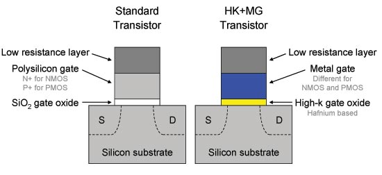
At 32nm the transistors are approximately 70% the size of Intel’s 45nm hk + mg transistors, allowing Intel to pack more in a smaller area.
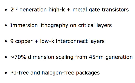
The big change here is that Intel is using immersion lithography on critical metal layers in order to continue to use existing 193nm lithography equipment. The smaller your transistors are, the higher resolution your equipment has to be in order to actually build them. Immersion lithography is used to increase the resolution of existing lithography equipment without requiring new technologies. It is a costlier approach, but one that becomes necessary as you scale below 45nm. Note that AMD to made the switch to immersion lithography at 45nm.
![]()
Intel reported significant gains in transistor performance at 32nm; the graphs below help explain:
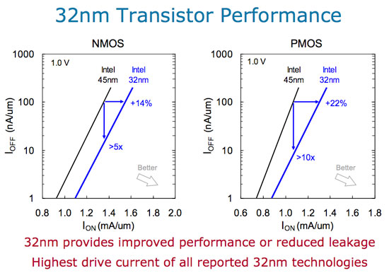
We’re looking at the comparison of leakage current vs. drive current for both 32nm NMOS and PMOS transistors. The new transistors showcase a huge improvement in power efficiency. You can either run them faster or run them at the same speed and significantly reduce leakage current by a magnitude of greater than 5 - 10x compared to Intel’s 45nm transistors. Intel claims that its 32nm transistors boast the highest drive current of all reported 32nm technologies at this point, which admittedly there aren’t many.
The power/performance characteristics of Intel’s 32nm process make it particularly attractive for mobile applications. But more on that later.


64 Comments
View All Comments
Targon - Wednesday, February 11, 2009 - link
For the CPU market, the problem is the ever growing amount of cache memory. Intel processors are designed with the large cache being their solution to improvements that AMD brings to the table.I suspect that Intel will have more trouble after this move to the new fab process because the difficulty in moving to a new process node grows at an exponential rate. We saw Intel hit a wall with the Pentium 3 line because they were not ready for a new process shrink at that point, so the P4 came out. When Intel got their process technology on track, the people at Intel could go back to the Pentium 3 design(with improvements) to release the Core and Core 2 Duo.
There will come a time when an all new design will be needed in order to hold on to their lead, and that is when AMD will probably catch back up, if AMD can survive until then.
BSMonitor - Thursday, February 12, 2009 - link
What an utter load of BS. Thanks fanboy.You get all that from wiki?
PrinceGaz - Wednesday, February 11, 2009 - link
Even though my last three CPUs were all from AMD (they made sense at the time- K6-III/400, Athlon XP 1700+, Athlon 64 X2 4400+), I have to disagree with your comment about the improvements (presumably the integrated memory controller) which AMD brings to the table.With Core i7, Intel has effectively removed the one last technological advantage AMD had- faster memory access. The fact that Intel chips still tend to have larger L3 caches is quite simply because they can afford to give it to them, as they are ahead of AMD on the fab-process. For a high-end desktop chip where there is die-space to spare, you could add some more cores which will probably sit idle (keeping four busy is hard enough, especially with HT), but adding more L3 cache (so long as the latency of it is not adversely affected) is a very cheap and easy way to use up the space and provide a bit of a speedup in almost everything.
AMD is currently fighting a losing game. The Phenom II (bug-fixed Phenom) cannot compete with Core i7 with AMDs current fabs, and unlike Intel who have the tick-tock steady new-process, then new-design with large teams working on each step; AMD seem to have one team working on a new design, which has to be made to work with whichever process looks like the best option at the time.
We need AMD to survive for the x86 (or x64, who came up with that :p ) CPU market to be competitive, but I think the head of AMD is going to have to get into bed with the head of IBM, else they are doomed to fall ever further behind Intel in chip-design. The K10 is promising, but a long way off still, and AMD hasn't exactly been raking in the billions of dollars of profits recently to do that R&D. VIA have found an x86 CPU niche they can compete in, I fear that unless AMD pull an elephant out the hat with the K10, they'll have to slot in between VIA and Intel in providing CPUs specialising in a particular performance-sector, with Intel being the undisputed leader.
JonnyDough - Wednesday, February 11, 2009 - link
Well said. I concur.