Conroe Buying Guide: Feeding the Monster
by Gary Key & Wesley Fink on July 19, 2006 6:20 AM EST- Posted in
- Motherboards
ASUS P5N32-SLI SE
Basic Features
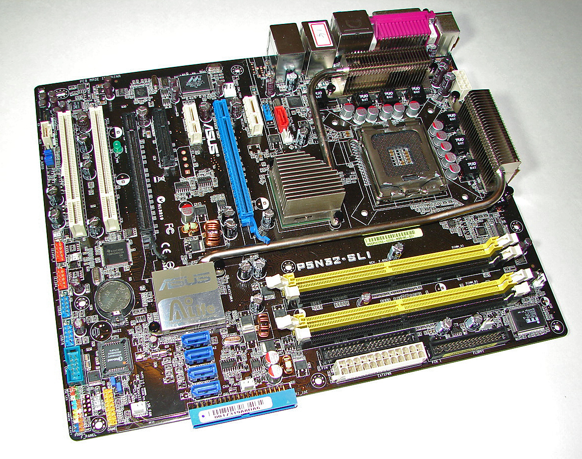
We reviewed the ASUS P5N32-SLI back in October 2005 in its initial release to the market. At that time the board revision and BIOS we tested with offered excellent performance, stability, and compatibility across the board. It was also the first Intel board to offer dual X16 support for NVIDIA SLI and with the right Pentium 4 or Pentium D processor the P5N32-SLI offered very good gaming performance.
Since that time the original board has either been loved or hated by its owners. Over the course of time the board was revised with changes to the resistors to improve VRM performance along with numerous BIOS revisions that just never lived up to the results of our pre-release 0047. Issues ranged from poorer than normally accepted FSB overclocking results with premium components, memory incompatibilities with 4GB installations, RAID issues with various BIOS releases, and other items that generally tarnished the reputation of the board.
ASUS did listen to the user complaints and additional component changes were made on the board to improve stability - but the most significant changes occurred in the BIOS. While the options generally remain the same, the overall performance of the board (along with stability) has improved over the previous 1.02 version of the board with the 0310 BIOS.
We are still testing the board with a wide array of components but we are glad - actually relieved - to report that the majority of user issues reported to us have been solved. The differences between the two boards are of course compatibility for the Core 2 Duo series, a couple of minor layout changes with the 4-pin 12V Molex connector being removed, and additional capacitors being added to the board for improved stability. The SATA ports are still in the same location which means SLI users will want to plug in their drives before installing the second video card. The basic features and layout of the ASUS P5N32-SLI SE remain nearly the same as the original board.
Basic Performance
Overall, the performance of the P5N32-SLI was excellent. It is also the only board in our Buyers Guide to officially support NVIDIA SLI. It not only supports SLI but offers full dual X16 capability to each PCIe graphics slot. The board was very stable with our X6800, E6700, and E6600 Core 2 Duo processors while providing asynchronous operation between the front side bus and memory controllers. This ability allowed us to dial in extremely low memory latencies at specific speeds in order to maximize the bandwidth of our Corsair DDR2 modules. Like the 975X boards, the nForce4 Intel Edition chipset allows the user to adjust the X6800 CPU ratios up or down.
This ASUS board had a tendency to get very warm during testing and requires a case with good air circulation to operate at normally accepted temperatures. Although the board never failed during overclocking or extended testing, our fingers on more than one occasion wanted to be iced down after touching the passive heatsinks on either the MCP or SPP.
We anxiously await the production release of the nForce 500 Intel Edition chipsets in a few weeks that will mainly bring benefits to the MCP such as additional SATA ports, improved networking features, HD Audio, and some general refinement. Users need to realize that the nForce 590 SLI Intel Edition will still use the C19A SPP will be used that is on this board. Although the chipset is now at a revision C1 and has undergone several months of fine tuning, do not expect the performance or overclocking results to be improved greatly with the nForce 590 SLI boards. In our internal testing we have noticed some minor but measurable improvements, but nothing revolutionary.
Overclocking
This is not the board to own if you expect or require high FSB overclocks with fixed multiplier Intel CPUs. While the FSB results are in alignment with other NVIDIA chipset boards they do not match overclocking results with Intel chipset boards at this time. We expect to see this change when NVIDIA releases their revised chipsets in several months. However, the board did match the overclock ranges of the Intel 975X board when increasing the multiplier on the X6800, and that allowed far greater control/tuning of the memory speeds due to the asynchronous operation of the controllers.
Although we wish the board provided additional memory voltage settings, we were able to run our memory timings at higher speeds with lower latencies than on the Intel chipset boards. That resulted in improved performance of the board when overclocked. Our only issue with the memory controller at this time is that the BIOS does not fully support memory timings over DDR2-1000 - although this should change before release. We will provide overclocked performance results in an upcoming article along with a comparison to the AM2 SLI boards. This board should sell in the $190 range, significantly lower than the first available Intel 975X boards with stock performance that matches or exceeds those boards. If dual X16 SLI is important to you and high FSB overclocks are not, then this is currently the board to have.
Basic Features
| ASUS P5N32-SLI SE | |
| Market Segment: | High-End/Enthusiast |
| CPU Interface: | Socket T (Socket 775) |
| CPU Support: | LGA775-based Pentium 4, Pentium XE, Celeron D, Pentium D, Core 2 Duo |
| Chipset: | nForce4 Intel SLI Intel Edition (C19 revC1) nForce4 Intel SLI Edition (CK-804) |
| Thermal Design: | 8-phase power Fan-less Heatpipe Cooling ASUS Stack Cool 2 for OC |
| Bus Speed Support: | 1066/800/533MHz |
| Bus Speeds: | 533 to 1600 in 1MHz Increments |
| Memory Speeds: | 400 to 1600 in 1MHz Increments |
| PCIe Speeds: | 100 to 148.4375 in 1.5625MHz Increments |
| PCI: | Fixed at 33 |
| AI Tuning: | Manual, Auto, Overclock Profile, AI N.O.S. |
| Core Voltage: | Auto, 1.2250V to 1.7000V in 0.0625V increments |
| PEG Link Mode: | Auto, Disabled, Normal, Fast, Faster |
| CPU Clock Multiplier: | Auto, 6x-20x in 1X increments if CPU is unlocked |
| DRAM Voltage: | 1.8V to 2.4V in .05V or .10V increments |
| 1T/2T Memory: | Auto, 1T, 2T |
| DRAM Timing Control: | Auto, 6 Options |
| NB HT: | Auto, 200MHz, 400MHz, 600MHz, 800MHz, 1000MHZ |
| SB HT: | Auto, 200MHz, 400MHz, 600MHz, 800MHz, 1000MHZ |
| NB Voltage: | Auto,1.4V, 1.5V, 1.6V |
| SB Voltage: | Auto,1.5V, 1.6V |
| Memory Slots: | Four 240-pin DDR2 DIMM Slots Dual-Channel Configuration Regular Unbuffered Memory to 16GB Total |
| Expansion Slots: | 2 - PCIe X16 1 - PCIe X4 2 - PCIe X1 2 - PCI Slots 2.2 |
| Onboard SATA/RAID: | 4 SATA 3Gbps Ports - NVIDIA 2 SATA 3Gbps Ports - SI3132 (RAID 0,1,0+1,JBOD) -NVIDIA (RAID 0,1) - Silicon Image 3132 |
| Onboard IDE: | 2 Standard ATA133/100/66/33 Ports (4 drives) |
| Onboard USB 2.0/IEEE-1394: | 10 USB 2.0 Ports - 4 I/O Panel, Six via Headers 2 Firewire 400 Ports by TI TSB43AB22A |
| Onboard LAN: | Dual Gigabit Ethernet Marvell 88E1115 PHY, Marvell 88E8053 |
| Onboard Audio: | Realtek ALC850 8-channel Codec |
| Power Connectors: | ATX 24-pin, 8-pin EATX 12V |
| I/O Panel: | 1 x Parallel 1 x S/PDIF Out (Coaxial + Optical) 1 x PS/2 Keyboard 1 x PS/2 Mouse 2 x RJ45 4 x USB 2.0/1.1 1 x External SATA 8-Channel Audio I/O |
| BIOS Revision: | AMI 0121 |
We reviewed the ASUS P5N32-SLI back in October 2005 in its initial release to the market. At that time the board revision and BIOS we tested with offered excellent performance, stability, and compatibility across the board. It was also the first Intel board to offer dual X16 support for NVIDIA SLI and with the right Pentium 4 or Pentium D processor the P5N32-SLI offered very good gaming performance.
Since that time the original board has either been loved or hated by its owners. Over the course of time the board was revised with changes to the resistors to improve VRM performance along with numerous BIOS revisions that just never lived up to the results of our pre-release 0047. Issues ranged from poorer than normally accepted FSB overclocking results with premium components, memory incompatibilities with 4GB installations, RAID issues with various BIOS releases, and other items that generally tarnished the reputation of the board.
ASUS did listen to the user complaints and additional component changes were made on the board to improve stability - but the most significant changes occurred in the BIOS. While the options generally remain the same, the overall performance of the board (along with stability) has improved over the previous 1.02 version of the board with the 0310 BIOS.
 |
| Click to enlarge |
We are still testing the board with a wide array of components but we are glad - actually relieved - to report that the majority of user issues reported to us have been solved. The differences between the two boards are of course compatibility for the Core 2 Duo series, a couple of minor layout changes with the 4-pin 12V Molex connector being removed, and additional capacitors being added to the board for improved stability. The SATA ports are still in the same location which means SLI users will want to plug in their drives before installing the second video card. The basic features and layout of the ASUS P5N32-SLI SE remain nearly the same as the original board.
Basic Performance
Overall, the performance of the P5N32-SLI was excellent. It is also the only board in our Buyers Guide to officially support NVIDIA SLI. It not only supports SLI but offers full dual X16 capability to each PCIe graphics slot. The board was very stable with our X6800, E6700, and E6600 Core 2 Duo processors while providing asynchronous operation between the front side bus and memory controllers. This ability allowed us to dial in extremely low memory latencies at specific speeds in order to maximize the bandwidth of our Corsair DDR2 modules. Like the 975X boards, the nForce4 Intel Edition chipset allows the user to adjust the X6800 CPU ratios up or down.
This ASUS board had a tendency to get very warm during testing and requires a case with good air circulation to operate at normally accepted temperatures. Although the board never failed during overclocking or extended testing, our fingers on more than one occasion wanted to be iced down after touching the passive heatsinks on either the MCP or SPP.
We anxiously await the production release of the nForce 500 Intel Edition chipsets in a few weeks that will mainly bring benefits to the MCP such as additional SATA ports, improved networking features, HD Audio, and some general refinement. Users need to realize that the nForce 590 SLI Intel Edition will still use the C19A SPP will be used that is on this board. Although the chipset is now at a revision C1 and has undergone several months of fine tuning, do not expect the performance or overclocking results to be improved greatly with the nForce 590 SLI boards. In our internal testing we have noticed some minor but measurable improvements, but nothing revolutionary.
Overclocking
| ASUS P5N32-SLI SE Overclocking Testbed |
|
| Processor: | Intel Core 2 Duo E6700 Dual Core, 2.67GHz, 4MB Unified Cache 1066FSB, 10x Multiplier |
| CPU Voltage: | 1.525V (default 1.2V) |
| Cooling: | Tuniq Tower 120 Air Cooling |
| Power Supply: | OCZ GameXStream 700W |
| Memory: | Corsair Twin2X2048-PC2-8500C5 (2x1GB) (Micron Memory Chips) |
| Hard Drive | Hitachi 250GB 7200RPM SATA2 16MB Cache |
| Maximum OC: (Standard Ratio) |
318x10 (4x HT, 3-3-3-9 1T) 3180MHz (+19%) |
This is not the board to own if you expect or require high FSB overclocks with fixed multiplier Intel CPUs. While the FSB results are in alignment with other NVIDIA chipset boards they do not match overclocking results with Intel chipset boards at this time. We expect to see this change when NVIDIA releases their revised chipsets in several months. However, the board did match the overclock ranges of the Intel 975X board when increasing the multiplier on the X6800, and that allowed far greater control/tuning of the memory speeds due to the asynchronous operation of the controllers.
Although we wish the board provided additional memory voltage settings, we were able to run our memory timings at higher speeds with lower latencies than on the Intel chipset boards. That resulted in improved performance of the board when overclocked. Our only issue with the memory controller at this time is that the BIOS does not fully support memory timings over DDR2-1000 - although this should change before release. We will provide overclocked performance results in an upcoming article along with a comparison to the AM2 SLI boards. This board should sell in the $190 range, significantly lower than the first available Intel 975X boards with stock performance that matches or exceeds those boards. If dual X16 SLI is important to you and high FSB overclocks are not, then this is currently the board to have.


123 Comments
View All Comments
Gary Key - Wednesday, July 19, 2006 - link
I am surprised I did not see this posted on a news site somewhere announcing Intel has a X6600. ;-) The line was corrected this morning to (X6800, E6700, E6600) although late last night my mind was probably thinking unlocked E6600 equals X6600 for some reason. Thanks for the notice! :)
drarant - Wednesday, July 19, 2006 - link
In recent months the memory market has moved from a 1GB kit to a 2BG kit being the common memory configuration.2GB*
Excellent article, I'm assuming the OCing results were default voltages on the chipsets and/or the cpu?
drarant - Wednesday, July 19, 2006 - link
page 11, 2nd to last sentence*Patsoe - Wednesday, July 19, 2006 - link
To be honest, I would say it's quite different!
The storage controllers have been changed a lot... there is now a port-multiplier type of SiI chip that connects to one of the ICH7 ports, which provides driverless (!) RAID. Also, the previous board had a Marvell SATA/PATA controller instead of the JMicron controller.
For another difference: the new board is missing the PCIe 4x slot, too.
Anyway, thanks for the great overview! And it's amazing how fast after launch you got this up.
Wesley Fink - Wednesday, July 19, 2006 - link
Thanks for your comment. We added information to the P5W-DH page with a little more info on the differences from the earlier board.nicolasb - Wednesday, July 19, 2006 - link
...is what is the actual impact on system performance of different memory speeds and timings? Possibly you guys actually derive a direct erotic thrill simply from knowing that your memory timings are 4-3-3-9 ;-) but what the rest of us care about is whether any given timings actually provide a tangible improvement to running applications. If I spend an extra £200 on memory, am I going to get an extra 10fs in a certain game, or just an extra 1fps if I'm lucky? That's what I want to know.Conroe is a new chip and it is by no means obvious (to me, anyway) whether the speed/latency of the memory will have a greater or lesser impact on the performance of the system than is the case for Netburst or A64 chips.
So, how about re-running some of your benchmarks on one particular board and producing results for different memory speeds and latencies?
Wesley Fink - Wednesday, July 19, 2006 - link
The original plan was to publish a Conroe memory article prior to this huge motherboard and memory roundup. The move forward of the Conroe launch by two weeks shifted our schedule quite a bit, as we discussed in the Buying Guide. we have found the timings DDR2 memory can achieve give a rough idea of the performance hierarchy on Conroe. That is 1067 at 4-4-4 is a bit faster than 800 at 3-3-3 is faster than 667 3-2-3. 667 is generally faster than nything slower regardless of timings.With 13 DDR2 kits it was impossible to do proper and complete performance testing on all the memory on Conroe and still deliver an article when you want to read it. There will definitely be followup reviews of memory on Conroe anwsering your questions in detail. We knew there would be complaints from some, but we also hoped you could understnad the roundup is posting 4 days after an early Conroe launch - and you can't even buy Core 2 Duo until 7/27 or later.
We wanted to provide solid info as soon as possible for those planning a Conroe purchase. We thought our finding that almost any Elpida value DDR2 will do DDR2-800 4-3-3 at about 2.2v was big news you would want to know, we will fill in the rest of the performance data as soon as we can.
As it is the roundup is over 15,000 words and one of the largest articles ever published at AT - in word length - and we really tried to be brief in each review. We really like giving our readers exactly what they want, but sometimes the realities of time and volume shift our priorities.
Tanclearas - Thursday, July 20, 2006 - link
Although I can understand what you're saying, maybe the following should not have been included in the introductory page.I guess the only surprise was that the comparison wasn't there. :P
Honestly, I tried to jump right to that section only to find rather useless comparisons of ridiculously expensive memory (which I won't buy) and "value" (read cheap) memory (which I won't buy). Also, can you really tell me that it was much of a surprise that the expensive memory all topped out at roughly the same speed (~1100, 5-5/4-5-15)? Nor am I particularly surprised the value memory could overclock reasonably well, but how about tests of the memory that I think most of your readers are likely to buy? I've been looking at DDR2, and you can get memory rated at DDR2-800 for a little more than the DDR2-667/533 variety, and still a lot less than the DDR2-1000 modules.
I know that you were pressed for time, especially with the launch being pushed forward. I just think (and it is only an opinion) that other tests should have been given priority over the ones you've completed.
kmmatney - Wednesday, July 19, 2006 - link
Also, what motherboard was used for the DDR tests? Often, value RAM is paired with a "value" motherboard. Value RAM may not look so well when paired with a value motherboard. I'm wondering how cheap we can go for reasonable peformance :)Gary Key - Wednesday, July 19, 2006 - link
We stated at the end of page 18 that we will be publishing performance results of the value memory roundup shortly. The amount of time required to test these seven modules at four different settings in several different applications was incredible and warrants a separate article update.