Intel Unveils Meteor Lake Architecture: Intel 4 Heralds the Disaggregated Future of Mobile CPUs
by Gavin Bonshor on September 19, 2023 11:35 AM ESTIntel Meteor Lake: Changing The Strategy, Laying the Foundation for Intel 3
The strategy for both the Intel 4 process and the first architecture built on it, Meteor Lake, looks to change the dynamic for the mobile market and the foreseeable future of Intel's client processors. With the Foveros 3D packaging, opting for a power-conscious mobile platform seemed the best way to showcase their gains in terms of power efficiency.
One of the main product assembly advantages of Foveros packaging is that Intel can chop and change tiles depending on the processor, which includes current technologies, I/O, graphics, and compute cores. This approach to 3D tiled packaging also means that it is theoretically easier to introduce new tiles with faster cores with higher IPC performance, new graphics processors, and newer I/O, such as Wi-Fi 7. With Foveros not limiting Intel to use a single, monolithic die, it allows Intel to use different manufacturing processes for each of the tiles and integrate them onto the silicon. This is prevalent with the compute tile being built on Intel 4, while the graphics tile in Meteor Lake is made using TSMC's N5 node. This flexibility is key to advancing innovation, customizability, and, of course, wafer yield.
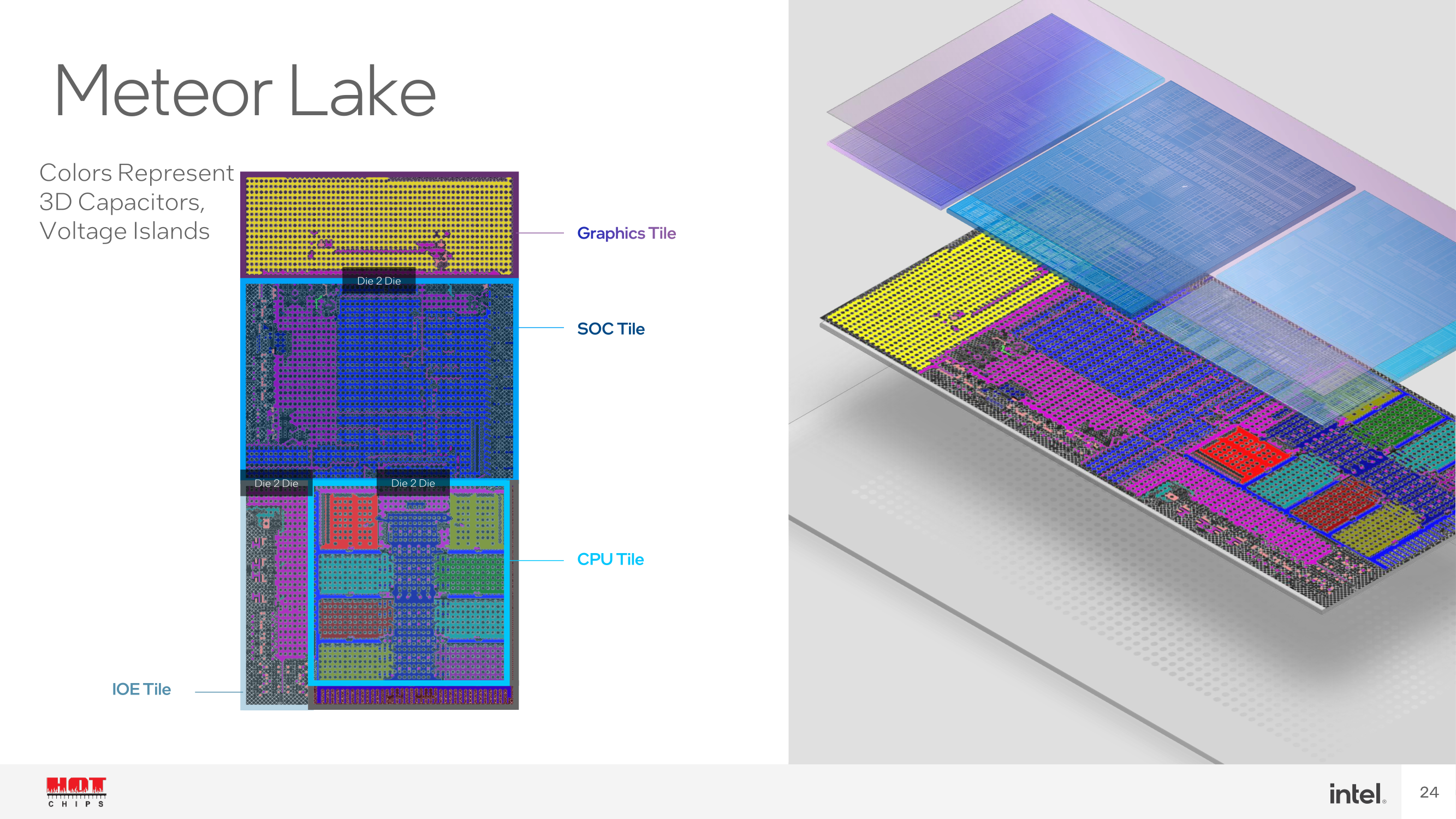
Intel Meteor Lake from Hot Chips Slide Deck
Intel also introduced a dedicated in-silicon AI engine through the NPU within the SoC tile. Similar to AMD with their Ryzen AI technology, Intel is looking to capitalize on the AI rush within its client-focused processors, but with support for OpenVINO and also including MCDM driver-compliance, users can do some pretty cool things with AI inferencing on the chip. Although these implementations aren't akin to the types of AI inferencing done in the cloud via ChatGPT with dedicated AI hardware, it's a step in the right direction in a world that looks to be slowly taken over by AI.
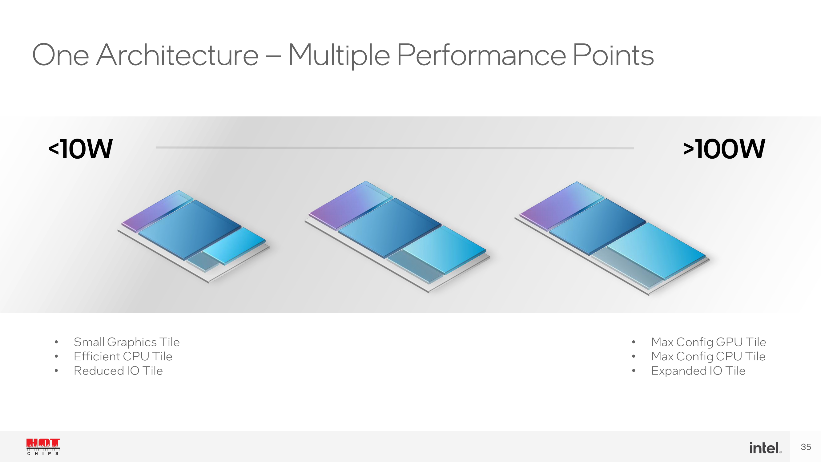
Wrapping things up, while Intel is confirming that Meteor Lake is coming to mobile-first, any details beyond that are slim pickings. At this point in time, Intel hasn't revealed anything in regard to SKUs or possible configurations. Everything disclosed is based on the 'full; Meteor Lake processors, but Intel hasn't spoken about different configurations or what the lower-end segment might look like regarding tiles and implementations. From their Hot Chips disclosures, offering a tiled architecture allows them to scale upwards and down depending on the SKU. The high-end SKU, which hasn't been disclosed yet, will feature the full configuration and implementation of all the features. Otherwise, the scalable nature of Meteor Lake and disaggregation allows for different levels of compute and graphics tiles and the ability to scale the input and output (I/O) depending on the device.
Meteor Lake will also be the first mobile platform from Intel to use their new Core naming scheme for products, which drops the 'i' from the Core branding. This includes the Core 3, 5, and 7, as well as higher spec Ultra 5, 7, and 9 Ultra tiers. Pat Gelsinger, Intel's Chief Executive Officer (CEO), during his opening keynote at Intel Innovation 2023, states that Intel is launching the first Meteor Lake Ultra (high-end) SKU with AI capabilities (NPU) on December 14th.

A tray of Meteor Lake Core Ultra processors (Credit, Intel)
We expect Intel to disclose more about specific SKUs and other specifications, such as clock speeds and core configurations, as we get closer to Meteor Lake's launch. Although we're expecting Ultra-focused Meteor Lake SKUs to launch on December 14th, no details on when we can expect other SKUs are set to hit retail channels. Meteor Lake is likely to launch with the top Ultra SKU or at least one that is close to the top of the stack.
Reading the tea leaves ahead of Innovation 2023, one gets the impression that Intel was hoping to be just a bit closer to launch by now than they actually are. But all things will eventually come in due time...


107 Comments
View All Comments
Composite - Thursday, September 28, 2023 - link
totally agree. At the same time, instead of doing a full Intel 4 Meteor lake chip, shrink it down to compute tile only also reduces the size of the silicon and improves yield. Later next year, Intel will also need EUV capacity for Sierra Forest and Granite Rapids. These chips will be much larger than mobile compute tile and considerably lower yield.... Intel will need every ounce of EUV capacity they have.tipoo - Tuesday, September 19, 2023 - link
Probably to have as much compute on the N4 capacity that they have, their substrate also takes much less power connecting them than current AMD and it allows for the best node for each part being used i.e if Intel's wasn't ideal for the GPU tile as the CPU tile etcComposite - Thursday, September 28, 2023 - link
I have the same question. At the same time, I was curious about Intel's EUV capacity. Since Intel is the late comer to EUV and over 50% of EUV machines are at TSMC, does Intel really have the capacity to manufacture full chip Intel 4 Meteor Lake? Not to mention up coming Sierra Forest and later on Granite Rapids will all use EUV capacity. I think the reasonable way is indeed only use EUV at the most critical part of Meteor Lake ---> Compute tile, and out source the rest.eSyr - Tuesday, September 19, 2023 - link
To avoid the issues they have with rollout 14 nm (BDW) and then 10 nm (CNL), I guess, when they held back by yield with respect to particular parts of the chip, specifically, GPU.lemurbutton - Tuesday, September 19, 2023 - link
A17 Pro just beat all Intel CPUs except the 13900KS in ST Geekbench6. A17 Pro uses less than 3w to achieve this - with typical load significantly below 3w. Meanwhile, 13900KS uses as much as 250w or more.Intel's Meteor Lake needs to improve by 10x over Raptor Lake just to match what M3 will be able to do.
Irish_adam - Tuesday, September 19, 2023 - link
The 13900ks uses 250 watts on a single core? Got a link for that?I'll think you find that single core workloads use far, far less. Also remember that benchmarks across ISA's are sketch at best and outright made up at worst. I mean just look how badly games or software can be when ported from one ISA to another, it all really comes down to how well you've made the software to run on each architecture.
Makaveli - Tuesday, September 19, 2023 - link
He is an apple fanboySource: Trust me bro!
FWhitTrampoline - Tuesday, September 19, 2023 - link
No the A17 Performance core is only clocked at 3.6/3.7GHz compared to the x86 designs that are up to clocked 2Ghz+ higher. So this is not some ESPN like Fanatic statement as since the A14/Firestorm core Apple's instruction decoder width is at least 8 decoders wide and backed up by loads of execution ports. And so Apple's P cores are of a very wide order superscalar design since the A14/Firestorm was released!And the Apple P cores are high IPC at low clocks compared to the x86 designs that have 4/6 instruction decoders so need the higher clocks to make up the IPC deficiency for single thread performance that's calculated as IPC multiplied by average sustained clocks to get that single threaded performance metric.
The lower clocks are where Apple's power savings come from and the longer battery life is obtained. That and the A17 Pro/Earlier A series SOCs have loads of specialized heterogeneous compute for offloading workloads onto instead of using the CPU cores or GPU cores so more power can be saved there for all sorts of specialized workloads. The x86 processors/SOCs are just now getting the same sorts of specialized heterogeneous compute IP blocks but that's relatively immature compare to Apple's SOCs and other ARM Based SOC ecosystems that have been using that specialized heterogeneous compute IP for years now.
GeoffreyA - Thursday, September 21, 2023 - link
Well, it would be interesting to see Intel or AMD make a fixed-width ISA design and how that then stacks up against the stuff of Apple. Really, x86 is at a disadvantage because of the variable-width instructions but still has done a fantastic job. Or, I'd like to see Apple design an x86 CPU and see how that holds up against Zen and the rest.FWhitTrampoline - Thursday, September 21, 2023 - link
No logical reason for Apple to go CISC as the x86 Instruction Decoder requires many times the transistors to implement than the transistors required to implement a RISC ISA Instruction Decoder! So it was easy to get 8 Instruction Decoders to fit on the front of the A14/Firestorm processor core(RISC ISA Based). It's easier to go wider if one has a relatively fewer Instructions of a fixed length to implement in a Instruction Decoder design. So that makes it easy to produce a custom very wide order superscalar processor core design that targets high IPC at a lower clock rate and the SOC's CPU cores clocked well inside their Performance/Watt sweet spot. And to still have that A14 match/get close to the x86 cores in single threaded performance and against x86 core designs that are clocked 2GHz+ higher.The x86 ISA is too Legacy Instructions bloated and it's not going to be easy to refactor that and not require years in the process to do that. The ARM ISA ecosystem is from the ground up RISC there and even though the x86 designers have a RISC like back end to break those CISC down into more RISC like instructions, that hardware engine take more transistors to implement and thus will use more power resources getting that done. The vast majority of ARM ISA instructions translate 1 to 1 into single and some a few Micro-OPs so how hard is that to decode compared to x86 ISA instruction that mostly have multiple micro-ops generated to get all that complex work done. And there's a valid power usage reason that x86 never made any inroads into the wider tablet/smartphone market.
The thing about the ARM/RISC core designs is that they can scale from phones to server/HPC whereas the CISC designs can not scale down as low power as RISC designs! but Intel has done a good job at getting close there but a little too late to matter to the OEMs that really did not want to remain beholden to Intel and x86. And the same can be said now for RISC-V compared to an ARM Holdings that's maybe leaning more towards an x86 like business model where RISC-V represents total end user ISA freedom there, within reason, as the RISC-V ISA is totally open not royalist/encumberments required/enforced.