Intel Unveils Meteor Lake Architecture: Intel 4 Heralds the Disaggregated Future of Mobile CPUs
by Gavin Bonshor on September 19, 2023 11:35 AM ESTGraphics Tile: A Generational Leap Through Arc, Xe-LPG Graphics
As part of their disaggregated architecture for Meteor Lake, Intel has opted to use a separate tile for graphics. Intel has gone down an interesting route for its disaggregated graphics, with the most notable inclusion through an upgrade to Intel's Arc Graphics architecture. Powering Intel's integrated graphics for Meteor Lake is a new graphics architecture which Intel calls Xe-LPG (and no, we're not talking about fuel here). Based on Intel's current discrete graphics architecture known as Xe-HPG (used in their Arc GPUs), Intel claims 2x performance per watt compared to the Xe-LP architecture-based Iris Xe integrated graphics within Intel's 12th Gen Core series.
There are a number of different elements within the graphics and media area of Meteor Lake, the bulk of which is built into the graphics tile, where the Xe-LPG graphics architecture is located. Unlike the compute tile (Intel 4) and the SoC tile, which is manufactured on TSMC N6 (6 nm), the graphics tile is made on TSMC's N5 node (5 nm), the same generational family as the nodes used by AMD and NVIDIA's discrete and integrated GPUs.
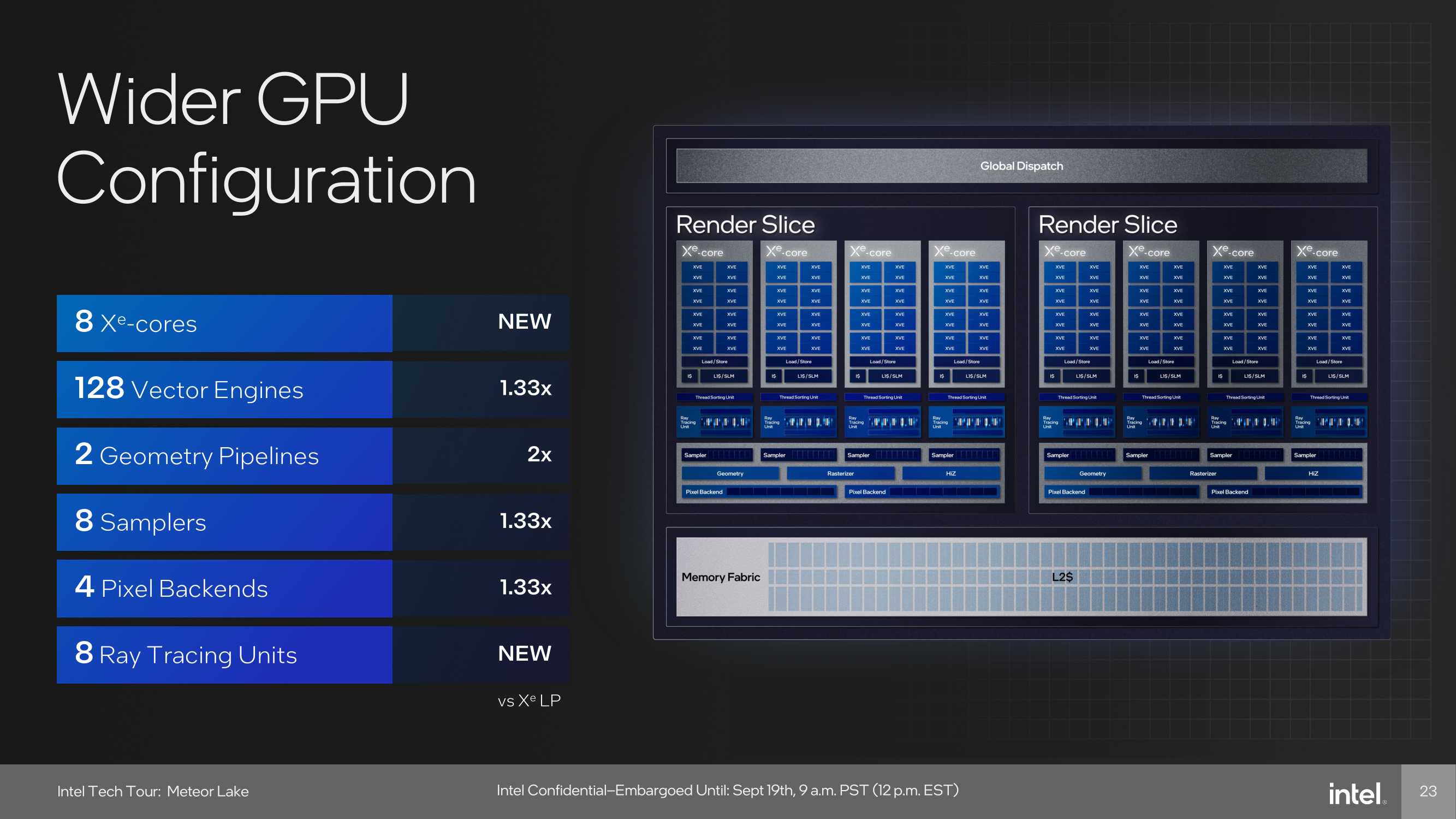
With Meteor Lake and the graphics tile with the Xe-LPG graphics processor, Intel is promising discrete-level performance in an integrated form factor. Looking at the finer specifications, Intel includes 8 x Xe graphics cores with 128 vector engines (12 per Xe core) and 8 samplers, representing a 1.33 x increase over Intel's previous Xe LP graphics. There are also 4 Pixel backends, which is an improvement over the 3 PBs on Xe LP. Intel also doubles the number of geometry pipelines within Xe-LPG, with two, and they also introduce 8 dedicated Ray Tracing Units (RTU), which is new for Intel's integrated graphics line-up.
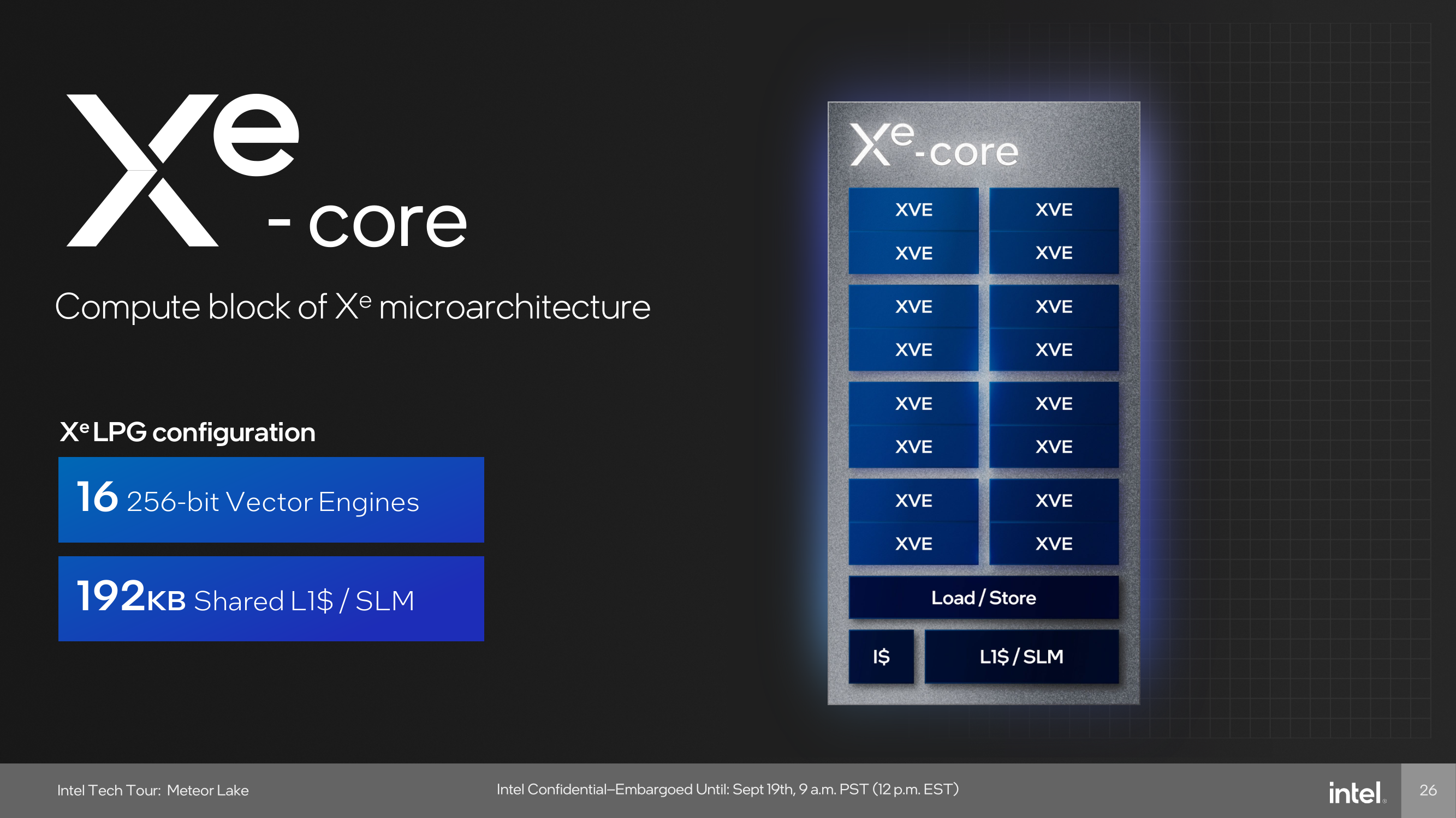
Looking at the makeup of Intel's Xe core, as previously mentioned, there are 16 Vector Engines that have a bus width of 256-bit, while each core also has 192 KB of shared L1 cache. Each Vector Engine enables 16 FP32 ops per clock, and 32 FP16 ops per clock, with a shared FP64 execution port with 64 INT8 ops per clock. One dedicated FP64 ops per clock unit is new over what's previously been seen in Raptor Lake and shares the overall design philosophy of Meteor Lake on power efficiency; pairs of Vector Engines can run in lockstep for better efficiency.
As part of Intel's goal of advancing the overall experience with Xe-LPG for users, the graphics are DX12 optimized, and Intel now brings Out of Order Samplng (OoOS) to Xe-LPG. It's worth noting that when talking about Execution Units (EUs), Intel's new and current term for this is Xe Vector Engines, or XVE for short. Intel hasn't provided us with how OoOS works within Xe-LPG, but we've reached out for more details.
| Comparing Intel Xe Integrated Graphics (Mobile) | ||||
| Meteor Lake (Xe-LPG) |
Raptor Lake (Xe-LP) |
Alder Lake GT1 (Xe-LP) |
Tiger Lake GT2 (Xe-LP) |
|
| Process Node | TSMC N5 | Intel 7 | Intel 7 | Intel 7 |
| Vector Engines/EUs | 128 | 96 | 96 | 96 |
| ALUs/Shaders | 1024 | 768 | 768 | 768 |
| TMUs | ?* | 48 | 16 | 48 |
| ROPs | ?* | 24 | 8 | 24 |
| Ray Tracing Units | 8 | - | - | - |
| TDP | ? | 15 W | 15 W | 15 W |
*Intel hasn't given us a deep dive into the finer specifications of Xe-LPG integrated graphics. Looking at an existing integrated Intel Arc equivalent with similar specs, the Meteor Lake Xe LPG could have 64 TMUs and 32 ROPs per the Arc A370M, which also has 1024 ALUs.
Comparing Intel's integrated Xe graphics from previous mobile architectures, Meteor Lake, through the Xe-LPG Arc based graphics, has 128 XVEs, which is an increase of 1.33 X or 32 XVE/EUs, than the previous Xe-LP generation. Regarding arithmetic logic units (ALUs), which are essentially shader cores, Xe-LPG has been increased to 1024, which is 128 ALUs per Xe-LPG core. As previously mentioned, Intel hasn't given us more about the finer specifications, including TMUs or ROPs, but does bring 8 Ray Tracing units, which is new for Xe-LPG when compared directly to Xe-LP.
Meanwhile, with Intel's Foveros 3D packaging technology, disaggregating the Media Engine and Display Engine from the graphics tile means when doing encoding or decoding, as well as video playback, it doesn't require the graphics tile to be powered up to do workloads on more power consuming cores.
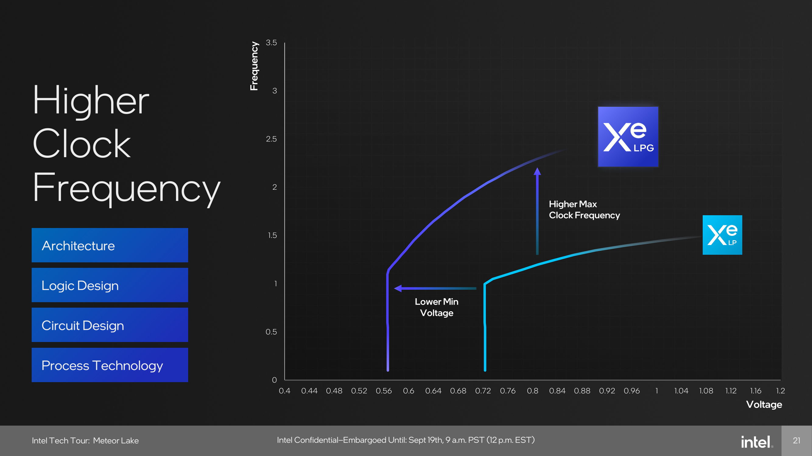
Intel Xe-LPG is the next step up from Xe LP, and one area where performance and efficiency gains are made is through a lower voltage frequency (V/F) curve, allowing the graphics to run at a lower minimum voltage with a higher maximum core clock speed. Intel has also optimized the pipelines for faster frequencies and is claiming up to 2 x performance at iso-voltages, which for a mobile platform such as Meteor Lake, adds more potential with a key focus on achieving a figure of up to 20% in power savings compared to the previous generation.


107 Comments
View All Comments
FWhitTrampoline - Thursday, September 21, 2023 - link
That would be more of DIY friendly Very Small Form Factor Enthusiast/end user there! And with a reasonable expectation that the vibrant DIY Small Form Factor devices(Mini desktop PCs) market continue to be offered Socket Packaged Processors with newer than Ryzen 5000G/Zen-3 and Vega 8CU iGPU based graphicsIP, and Ditto for any Intel based options as well.
So it's wrong to expect any Further Ryzen G series Desktop[Socket Packaged] APUs from AMD because that's not good for the OEMs there and their business models that are not so DIY friendly for Processor Upgrades if the Processor comes BGA wedded to the Motherboard! And OEM products that are not so good for eWaste reduction because if the processor goes that can not be easily replaced/upgraded by the end user(DIY sorts of Folks).
There needs to be a Right to Processor Upgrade just as much as a Right to Repair and with Socket packaged processors those rights go hand in hand there along with any environmental eWaste concerns. But we must not trample upon those Business Models as that's just not good for OEM Profits there, consumers be damned!
And InWin Chopin or ASRock Desk Mini, Socket Packaged APUs/SOCs are the best option as that's by definition DIY friendly there.
I'll expect no Complaints from you if the entire PC market goes BGA Packaged Processors only and you'll have to buy the Processor Attached to the Motherboard, take it or leave it!
brucethemoose - Wednesday, September 20, 2023 - link
> That might make a really nice media playerSeems like a lot of silicon for what's essentially the job of a dirt cheap ARM SoC. And its a questionable fit for a headless system unless its like a stable diffusion/transcoding host.
It *does* seems like an interesting fit for a smart TV chip, maybe with a small GPU die, as they would actually use the NPU for their internal video filtering.
emvonline - Tuesday, September 19, 2023 - link
Intel 4 will not be shipping any products to customers until Mid December. This after stating it is in production in December 2022. 12 months from production starts to PCs out is not good. And I better be able to buy meteor lake Notebook on Dec 14th 2023 or this is exactly like old Intel (Launch means we may have sold some parts to someone somewhere). This claiming a node is done when its production ready, when you ship nothing is problematic. FYI Meteor Lake is 2x the cost of Raptor lake in 2024. Intel 4 is not a cost reduction. The product might be great but it is expensiveRoy2002 - Tuesday, September 19, 2023 - link
4 was in production in December 2022? No way! It should be started not long ago.Usually the first real product silicon would be taped out one year ahead of release date. And that silicon would be very buggy and needs several steppings to have bugs fixed.
Roy2002 - Tuesday, September 19, 2023 - link
So December 2022 is the initial project tapein date and silicon debug follows.ChrisGar15 - Tuesday, September 19, 2023 - link
Probably called "manufacturing ready."xol - Wednesday, September 20, 2023 - link
So Xe-lpg is still intel uhd graphics (13\14th gen now?) with top EU count of 128 up from 96. Fine.maybe about 3TF fp32, not quite xbox Series S level
They added RT support which is good i guess but will it ever be used in a gpu that is really PS4 performance?, or maybe there are not gaming applications.
product sounds good, just wait for the numbering scheme
JBCIII - Wednesday, September 20, 2023 - link
"An example of how applications pool together the various tiles include those through WinML, which has been part of Microsoft's operating systems since Windows 10, typically runs workloads with the MLAS library through the CPU, while those going through DirectML are utilized by both the CPU and GPU."This sentence is really a mess. Editor: please take note. Is "example" the subject of "include"? That would make "includes" the necessary form of the verb. What is the subject of "runs"? I'm guessing WinML. Maybe it should be "WinML...which typically runs" but the long parenthetical expression about Windows 10 support makes it hard to bridge the gap. Maybe parentheses would be more clear instead of commas to keep the meaning on track. I'm still not sure what was meant.
GeoffreyA - Thursday, September 21, 2023 - link
WinML is the higher-level abstraction, and DirectML, the lower-level one.Kevin G - Wednesday, September 20, 2023 - link
This is what I was hoping to see Intel pull off in the late 14 nm/early 10 nm days when their foundries were having difficulties. Intel should have pivoted int his direction at the first sign of trouble with those as the packaging side of this, while cutting edge back then, could have been pulled off. Better late than never.However with Meteor Lake around the corner, it is shaping up to a pretty good design. Both the CPU and GPU sides can scale and evolve independently from the central SoC. The GPU portion that was moved onto the SoC makes sense as the codecs and display logic are not going to change over the next few generations. I would quibble about the point made that putting them next to the NPU is more advantageous than next to the GPU cores. There certainly is a benefit for AI upscaling of movies but my presumption is that I'd be lower power/lower latency to have the encoders next to the GPU cache which houses the final render frame for encoding and transmission. The tasks that's benefit here would be gaming streaming or remote access. Both things can be true hence why it is a quibble as it'll matter to individual use cases which one approach is superior.
My initial presumption for the IO die was that it was to house various analog circuits that would then be leveraged by the SoC die. This is a clever means of process optimization as analog circuitry does not scale at the same rate as logic. Similarly this would permit a cheaper die to extend the number of area intensive IO pads.
The last thing missing is the L4 cache die that was hinted at in earlier Linux patches. That'll probably come along with the Lunar Lake generation.