Voltage Lockdown: Investigating AMD's Recent AM5 AGESA Updates on ASRock's X670E Taichi
by Gavin Bonshor on May 16, 2023 12:00 PM EST- Posted in
- CPUs
- AMD
- ASRock
- Motherboards
- X3D
- Ryzen 7000
- X670E Taichi
- AGESA
AGESA 1.0.0.5c to 1.0.0.7: Differences With ASRock's X670E Taichi Firmware
Before we head into the testing, we figured it would be a good idea to highlight what we found different (if anything) within the BIOS of ASRock's X670E Taichi motherboard when updating the firmware from each successive version. Although nothing has changed from a GUI perspective, we can at least see some of the main settings that ASRock is presetting once AMD's EXPO memory profiles are enabled.
Screenshot of ASRock X670E Taichi UEFI firmware: BIOS 1.18 (AGESA 1.0.0.5c)
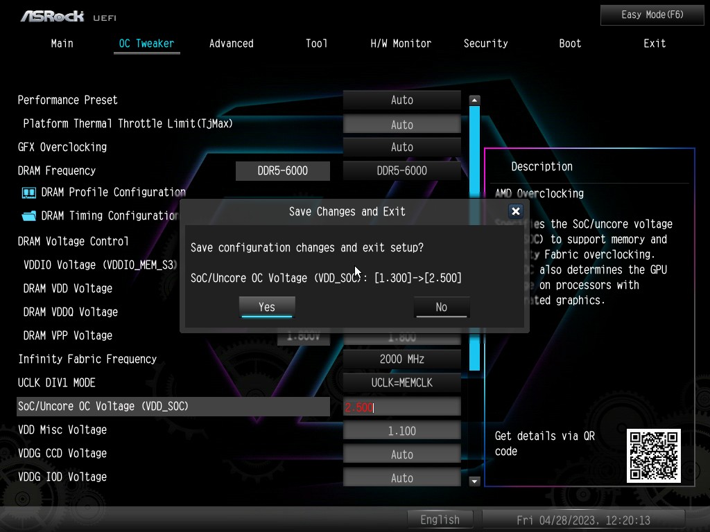
While nothing has changed in regards to the GUI, the most significant change from going from AMD's initial Ryzen 7000X3D-enabled BIOS is that users were able to set crazy levels of SoC voltage; the X670E Taichi would let us put 2.50 V on the SoC, which is ridiculously dangerous. As a reminder, the Ryzen 7000X3D chips are non-overclockable from a core frequency and VCore perspective, though they do support AMD EXPO memory profiles.
ASRock is clearly overshooting SoC voltage to ensure stability for users. When applying AMD EXPO on supported DRAM, all of ASRock's X670E Taichi firmware variants from AGESA 1.0.0.5c to the latest BETA AGESA 1.0.0.7 (BETA) variant, the firmware would automatically apply 1.30 V to the SoC voltage, regardless of what memory frequency is used. If users opt for a lower spec kit such as DDR5-6000 with EXPO, applying 1.30 V is a little overkill, as we found it made no difference to stability until we went below 1.25 V on the SoC voltage.
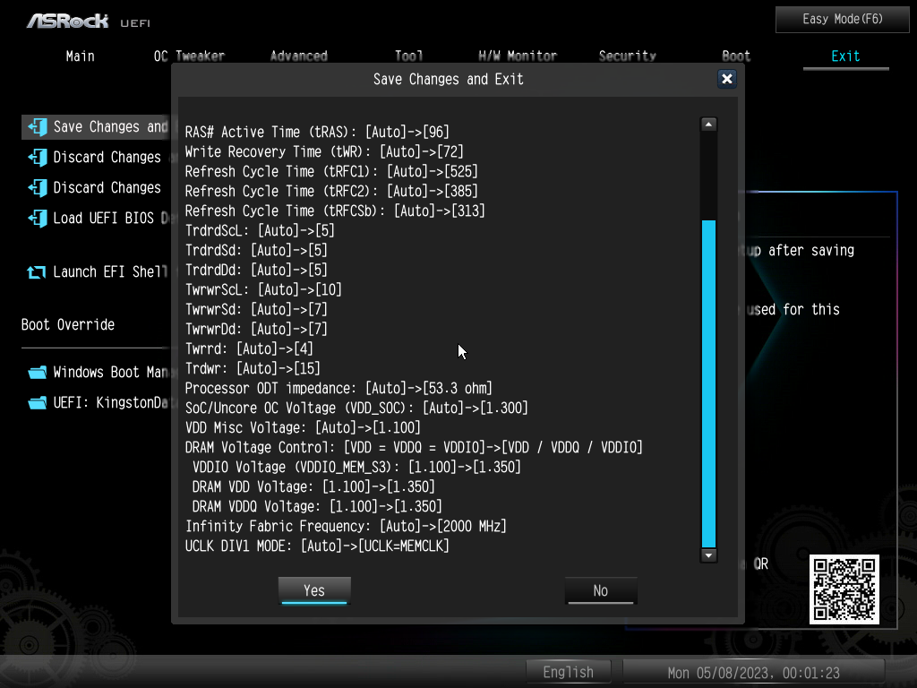
ASRock X670E Taichi firmware applying changes when using EXPO on our DDR5-6000 EXPO kit.
Looking at the changes that applying memory with an AMD EXPO profile has on the settings, we can see that ASRock automatically changes some key voltage settings relating to SoC, VDDIO, DRAM VDD, and DRAM VDDQ. As we previously mentioned, ASRock automatically applies 1.30 V to the SoC voltage when you use EXPO memory profiles, or even XMP 3.0 profiles, as we found out. The VDD misc voltage was set to 1.10 V from auto, with the DRAM voltage (DRAM VDD/VDDQ) increasing to 1.350 V from 1.10 V. As per the memory specifications and how AMD's Infinity Fabric works, the firmware automatically applied 2000 MHz for Infinity Fabric and changed the UCLK DIV from auto to equal the MEMCLK.
AMD AGESA 1.0.0.5c Up to 1.0.0.7: Analysis, Testing For Differentials
For our analysis of the changes that AMD's updated AGESA firmware has on specific variables when put under heavy and intensive memory-focused workloads, we'll be splitting the sections into two; memory at the JEDEC default specifications (settings on auto) and with EXPO enabled (DDR5-6000 CL34).
G.Skill Trident Z5 at DDR5-5200 (JEDEC) Settings
The key variables we'll be focusing on include the following:
- Peak Temperatures across the CPU die, CPU CCD1 (3D V-Cache), and CPU CCD2 (in °C)
- Peak Voltages including CPU VDDCR/VDD, CPU VDDR_SoC (SoC Voltage)
- Peak Current, including CPU Core current and SoC current (in amps)
- Peak Power, including CPU PPT (from the AM5 socket) and SoC power
In our results, the CPU die temp max average is an average of both CCD1, CCD2, core temperatures and L3 cache temperatures. This isn't to be confused with the average of the CPU die temp average.
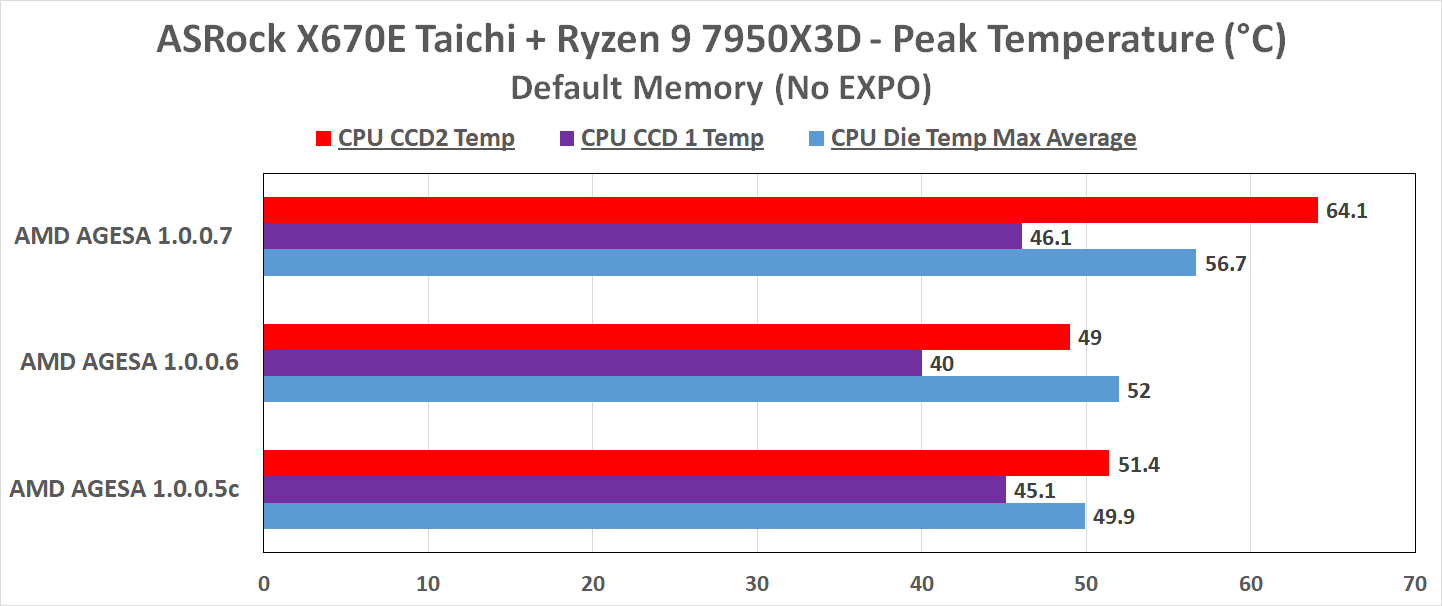
Starting with peak temperatures across both CCDs and the die, going from AGESA 1.0.0.5c to AGESA 1.0.0.7 (BETA), we can see that the CCD2 (non-V-Cache) was noticeably higher by just under 25%. The CCD (1) with 3D V-Cache was relatively consistent regarding peak temperatures, with a jump of just 2%. Overall, the CPU die temp, as with CCD1, was higher due to the different core temperatures on CCD2.
We can see that going to AGESA 1.0.0.6 from 1.0.0.5c resulted in slightly lower temperatures across all of the CCDs and overall die temp, but the latest AGESA 1.0.0.7 (BETA) (at the time of writing) was the hottest of all. One possible reason for the higher temperatures on AGESA 1.0.0.7 is that reducing power from the one component of the CPU, in this case, the SoC allows the actual Zen 4 cores slightly more headroom in terms of power.
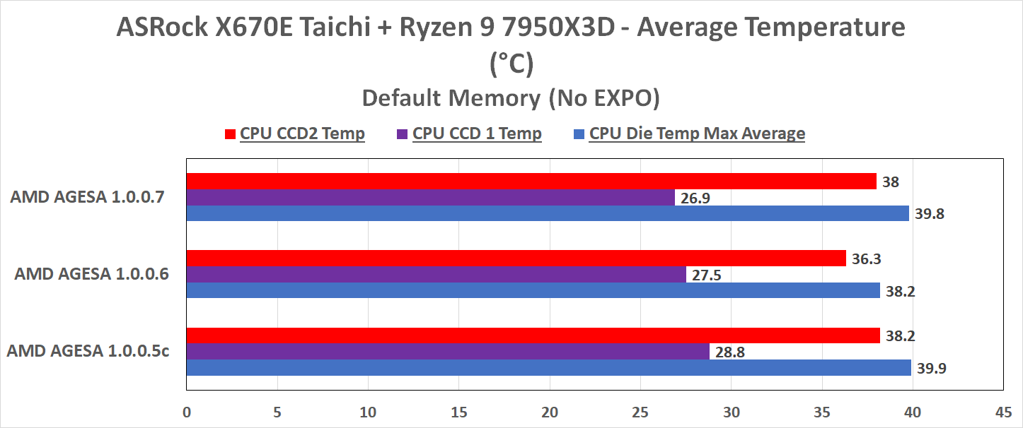
Looking at the average temperatures across CCD1 and CCD2 and the overall die temperature, we can see that there wasn't much variance between the different AGESA versions. Even on AGESA 1.0.0.7 with a higher temperature peak, the average is much more in line with the other AGESA versions.
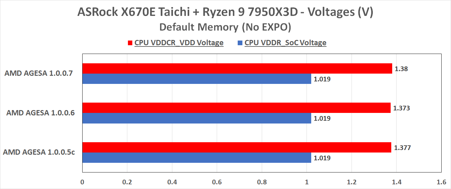
Focusing on voltages, including CPU VDDCR_VDD (memory voltage) and CPU VDDR_SoC voltages, we can see they are consistently within acceptable margins. While we're not focused on CPU VCore as it's well within specification, and hasn't been an issue as the Ryzen 7000X3D series chips are core frequency/voltage locked, the SoC and memory voltages are well within expected levels in line with our G.Skill Trident Z5 Neo DDR5-6000 memory's specifications.
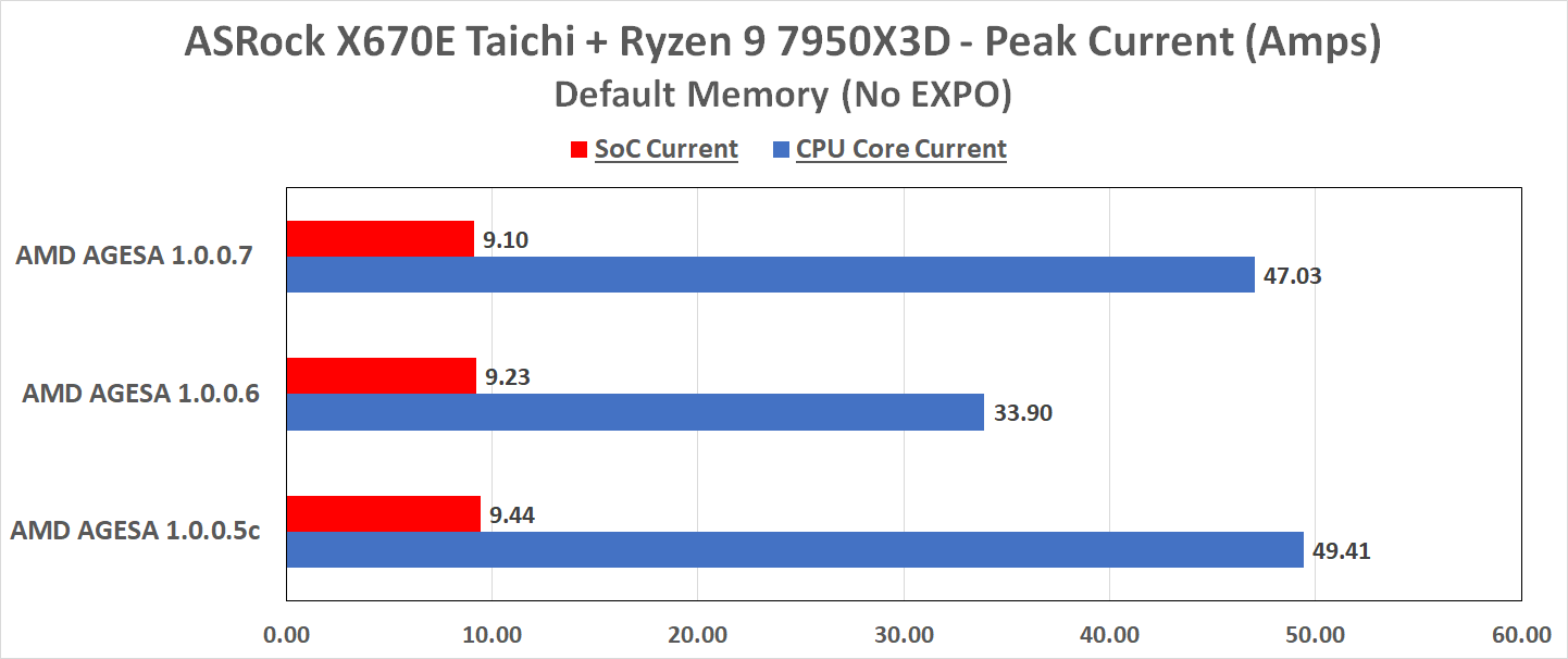
Although we observed higher temperatures across the board on AGESA 1.0.0.7 (BETA) without AMD's EXPO enabled, we can see that AGESA 1.0.0.5c's current peaked higher. While sustained current and voltages can spike higher than the averages, they aren't sustained and shouldn't be of concern, at least not from our testing.
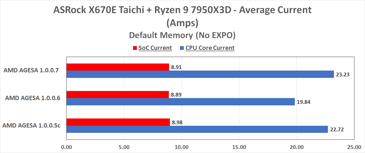
Focusing on the averages of both the SoC and CPU Core currents, we can see that AGESA 1.0.0.6 is slightly more reserved than the initial Ryzen 7000X3D series launch firmware and the latest AGESA 1.0.0.7 (BETA).
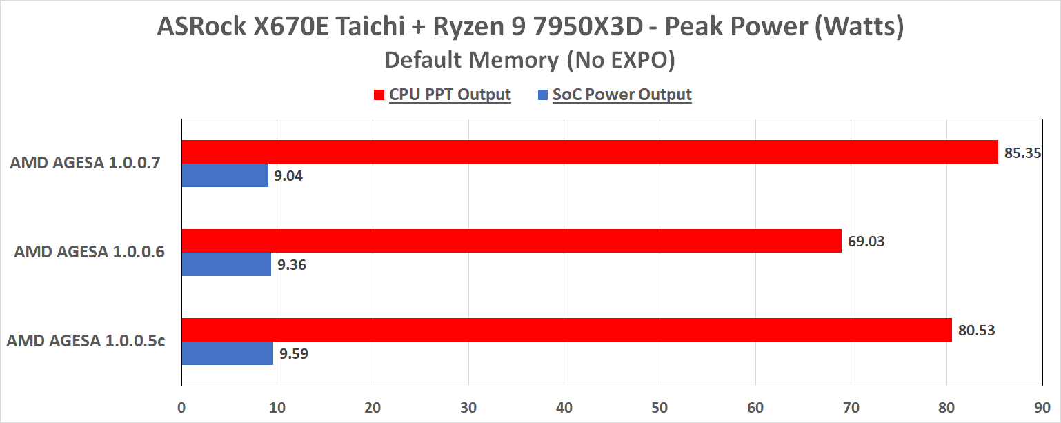
The actual power values monitored using HWInfo show that AGESA 1.0.0.7 (BETA) has a higher peak power from the socket (PPT) than the two other AGESA versions. As we've seen from our testing, AGESA 1.0.0.6 with our ASRock X670E Taichi is more conservative on current and power, so temperatures are lower across the board. Pulling more power from the socket with AGESA 1.0.0.7 (BETA) and our Ryzen 9 7950X3D does explain why temperatures are higher, both at peak and average.
Our testing shows that AMD's AGESA 1.0.0.7 (BETA) is consistent with other AGESA firmware versions at default memory settings. Still, we can see an increase in power draw and temperatures, at least on the ASRock X670E Taichi.
G.Skill Trident Z5 at DDR5-6000 (EXPO Enabled) Settings
Now onto our testing with the AMD EXPO memory profile enabled on our G.Skill Trident Z5 Neo DDR5-6000 CL34 kit. We've added another variable, with our DDR5-6000 kit also running with an applied SoC voltage of 1.25 V in the firmware.
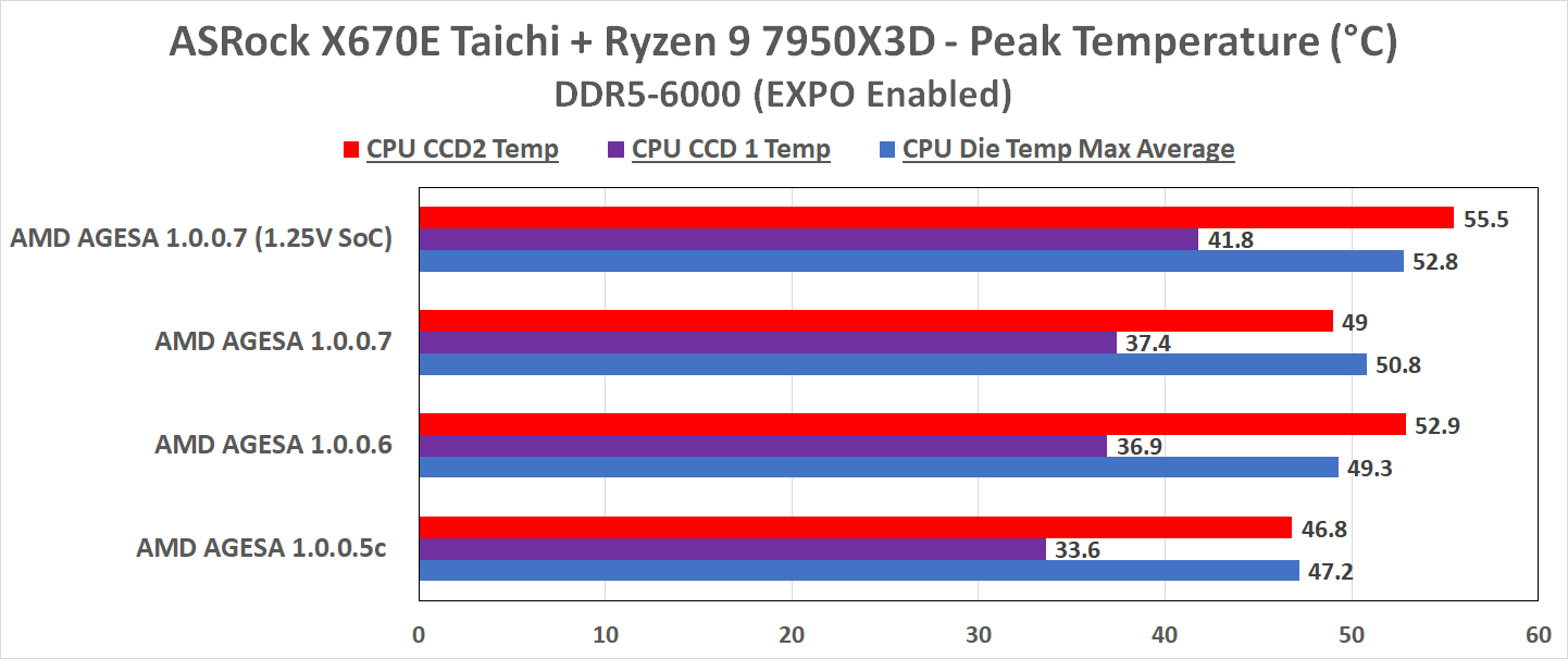
A closer look at peak temperatures shows a slight variation between all three AGESA firmware variants. Using AMD AGESA 1.0.0.7 (BETA) with 1.25V on the SoC voltage, CCD2 peaked at 55.5°C, the CCD without the 3D V-Cache. This was a noticeably higher spike than expected, given that SoC voltage was inherently lower than the other runs (1.30 V on the SoC).
Interestingly, the initial launch BIOS (AGESA 1.0.0.5c) for Ryzen 7000X3D processors ran with the lowest temperature on CCD2, and we observed the lowest spike in temps on CCD1 (3D V-Cache) too. Looking at the maximum CPU die temperature average, all were within quite acceptable margins, with nothing noteworthy in this regard and nothing out of the ordinary.
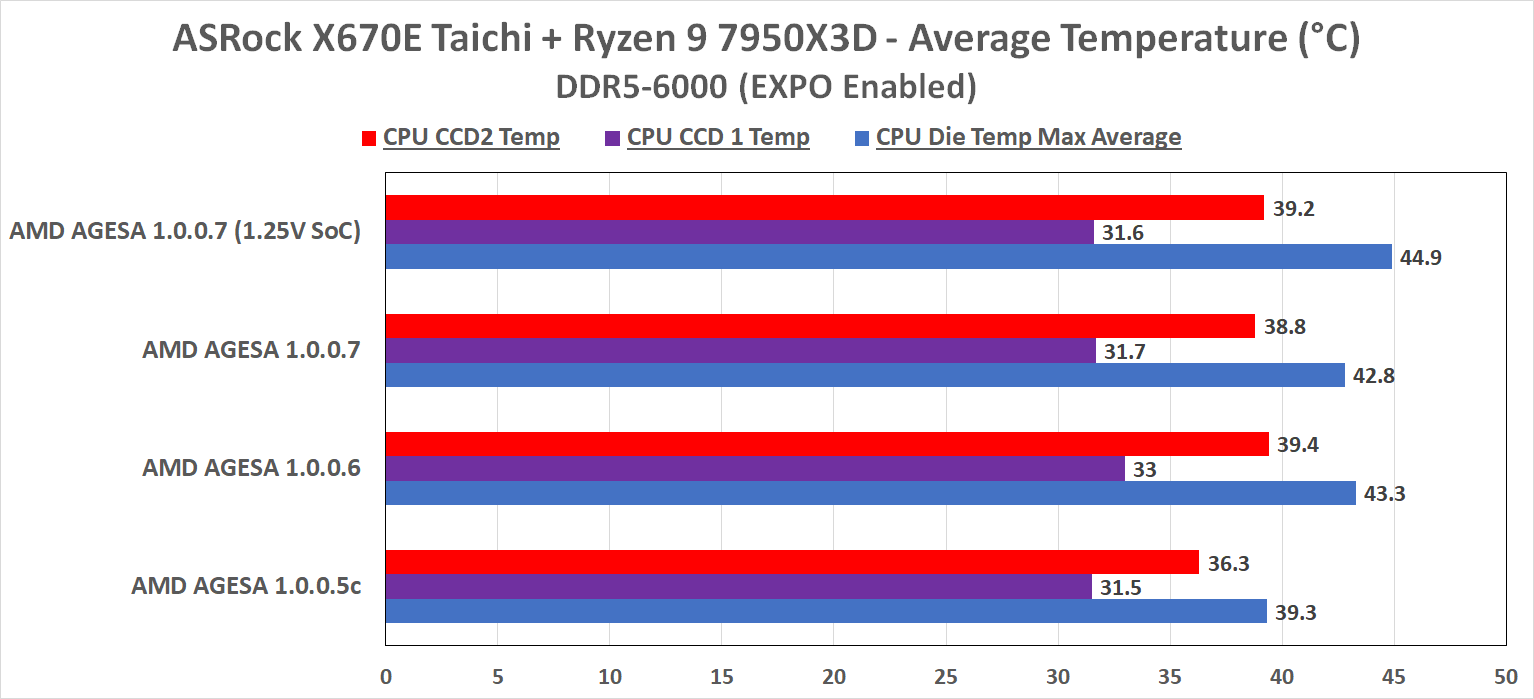
Moving to the average temperatures, we see things are much more balanced between the three AMD AGESA firmware versions. AGESA 1.0.0.7 (BETA) at 1.25 V on the SoC voltage still averaged slightly warmer on the non-3D V-Cache enabled CCD than on AGESA 1.0.0.5c, which was less on average compared to AGESA 1.0.0.6.
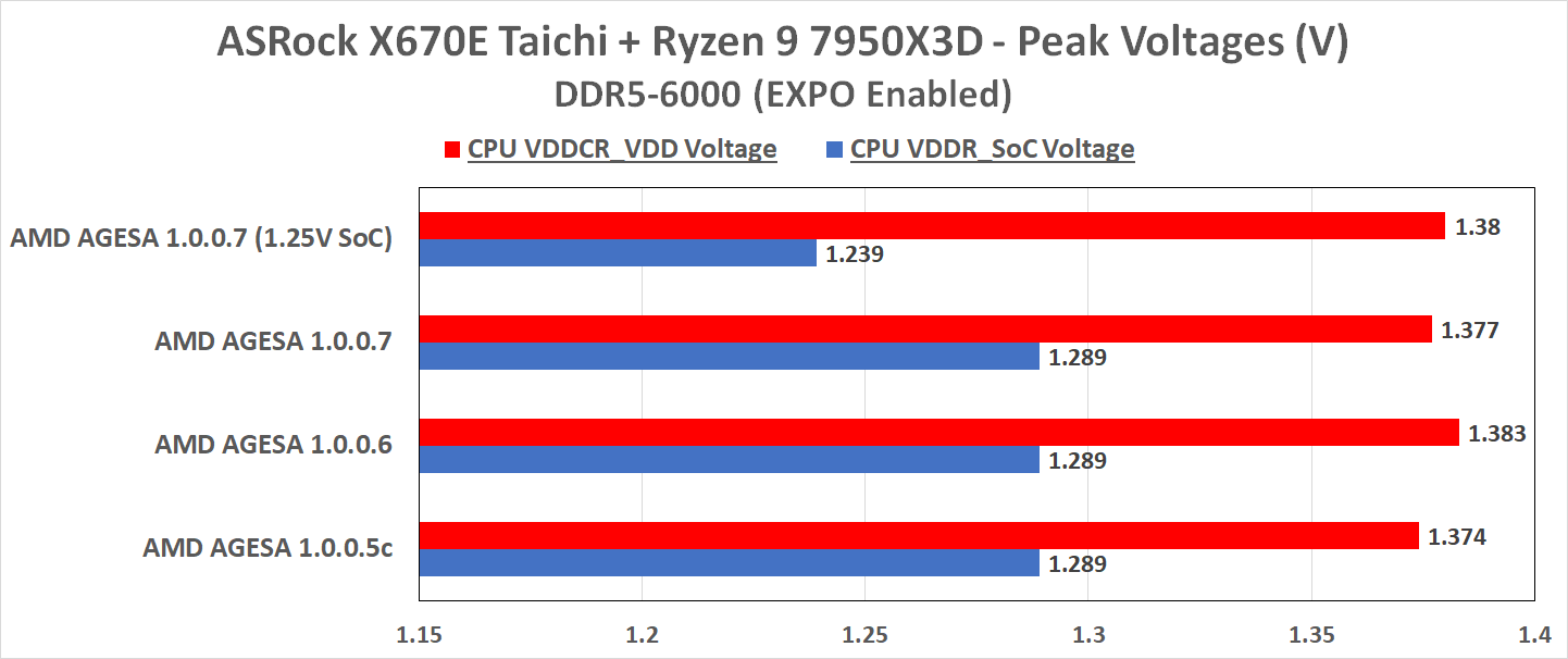
Concentrating on peak voltages across both the memory and CPU SoC voltages, we can see that AMD AGESA 1.0.0.6 peaked slightly higher on memory voltage than the other revisions. SoC voltage is consistent across all three AGESA variants at 1.289, showing that ASRock's firmware automatically setting 1.30 V for SoC is working well. At 1.25 V on AGESA 1.0.0.7 (BETA), our SoC voltage reading topped out at 1.239 V, which shows a bit of negative VDroop, a positive in this case.
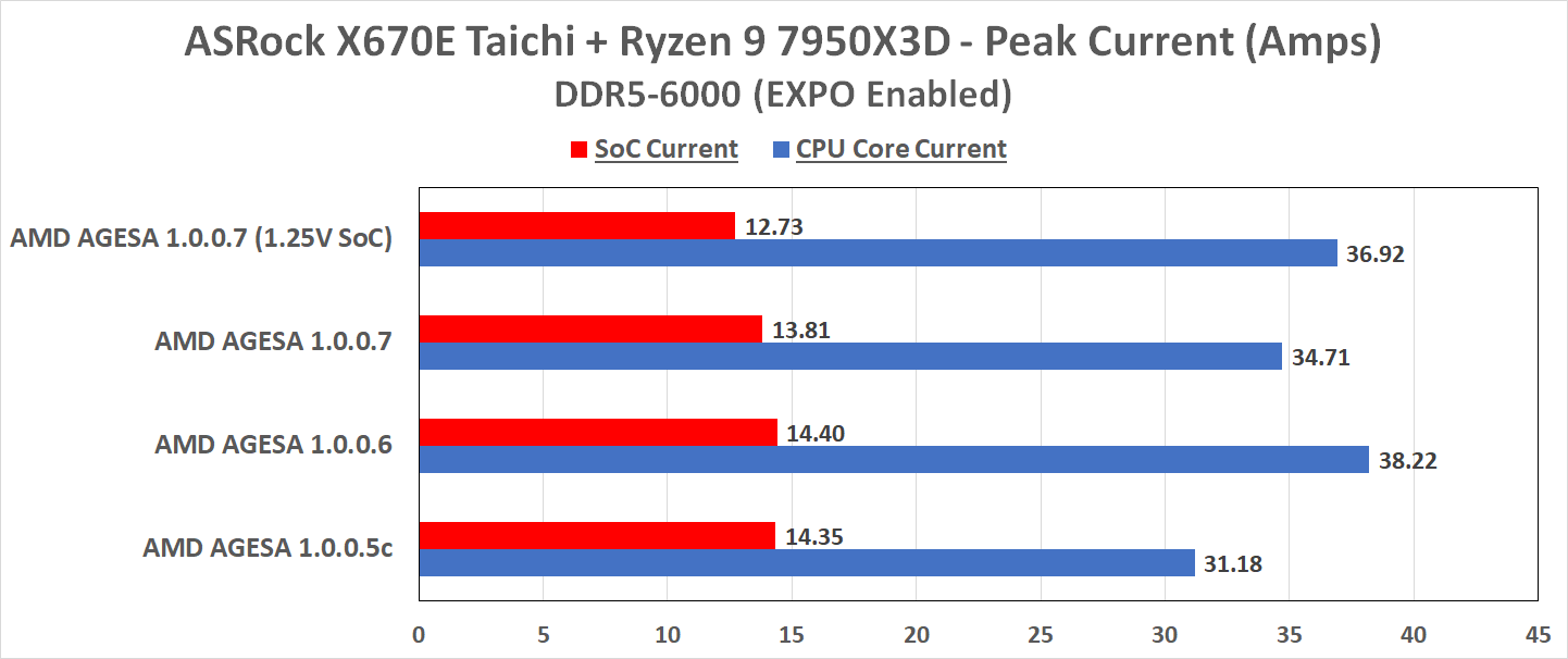
Again, AGESA 1.0.0.6 is operating with more courage as it pulls more amps than other versions; it's interestingly peaking at a higher current on the SoC voltage than the firmware before it, AGESA 1.0.0.6. It would have been thought that AMD's quick fix BIOS to address SoC voltages would peak at lower variables, and it peaks around half an amp higher than the latest AGESA 1.0.0.7 (BETA) firmware.
Even setting 1.25 V on the SoC, the amperage pulled from the rail responsible for the SoC is lower than 1.30 V, which is expected as less power is fed through it. Although we didn't experience any reported problems in our testing, CPU core current spiked higher on AGESA 1.0.0.6 than the other versions.
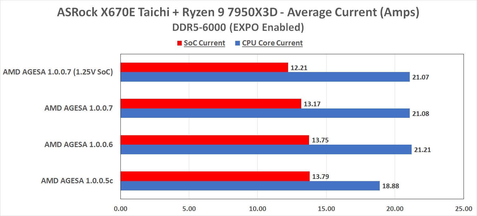
Focusing on average amps drawn from the SoC, things on the SoC balance back to expected levels, although there is not much variation comparing all three AGESA firmware. On average, with AGESA 1.0.0.6 and 1.0.0.7, we can see that the average CPU core current is noticeably higher than AGESA 1.0.0.5c, which is the initial launch BIOS for the X670E Taichi for Ryzen's 7000X3D series.
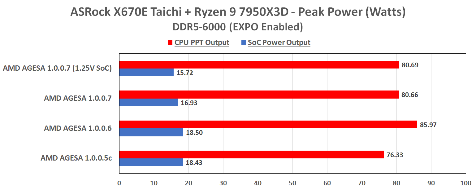
Lastly, the peak power output with AMD's EXPO memory profile enabled on our Ryzen 9 7950X3D with the ASRock X670E Taichi. As we can see, AMD AGESA 1.0.0.6 peaked out over 5 W higher on the AM5 socket than the other versions, and AGESA 1.0.0.5c seems to be the most conservative regarding this. For SoC power output, AGESA 1.0.0.6 spikes higher on power than the different versions, which could be one of the reasons that AMD replaced AGESA 1.0.0.6 so quickly.


39 Comments
View All Comments
Golgatha777 - Tuesday, May 16, 2023 - link
I'm on a B650E-F with a 7700X CPU. With all that's gone on here with the X3D parts, I think I'll give it awhile to sort things out before I think about upgrading to the 7800X3D. I upgraded to 1406 when I first got my motherboard, and I believe was the first one with X3D support (until ASUS started daily edits of their BIOS and CPU support lists anyway). I have a very stable system, so I plan to sit on the sidelines and not upgrade my BIOS until there's a non-beta one that's been listed for at least a couple of months.GreenReaper - Saturday, May 27, 2023 - link
I think if it was actually damaged it would have likely shown up in improper working. Most of the damage seems to have been people manually increasing SoC voltage, being allowed to do so.The_Assimilator - Tuesday, May 16, 2023 - link
This embarrassing disaster is the cherry on top for the dismal and disappointing Zen 4 launch. AMD managed to replicate the original Zen's rubbish memory controller, but this time around they "fixed" it by allowing board partners to overvolt it through the roof - with the inevitable result. Play stupid games, win stupid prizes.Sunrise089 - Tuesday, May 16, 2023 - link
I’ve vaguely followed this story but am obviously still somewhat out of the loop.I appreciate this article, but it seems like the conclusion here could be “ASRock boards don’t suffer from the overvolting issue,” no?
So what IS the real issue here? Is it just that Asus had bad voltage settings applied when users used faster memory? And that Asus just assumed they’d be fine because AMD would have protections in the chip that would prevent damage?
Is there more to it than that? Because otherwise I don’t understand why this is being presented as a general issue affecting AMD and multiple board partners if it’s really only Asus-specific.
meacupla - Wednesday, May 17, 2023 - link
There is more to it than that, yes. The older BIOS allowed 7000X3D to be overvolted when XMP was enabled. Asus was the most egregious, but this same flaw seems to have existed on all vendors.Asus mobos had a fail safe that didn't kick in properly.
It seems that AMD chips also don't have a fail safe that kicks in properly either.
AMD and mobo makers endorse fast RAM speeds, but AMD only "officially" supports DDR5-5200.
To ensure maximum RAM compatibility, Asus likely pushed Vsoc too high to get DDR5-6000 to 6400 to work on their mobos.
A high delta between Vsoc and Vram has resulted in poor RAM stability on the AM4 platform, and probably also does so on AM5, but that is just my guess.
Targon - Friday, May 26, 2023 - link
There is a difference between allowing the user to do stupid things, and the BIOS by default doing stupid things. This goes back to the old idea of AMD having supported freedom by allowing motherboard makers to tune things themselves, but when those motherboard makers completely screw up and don't even read the, "you shouldn't go over 1.3V" guidance, causing things to go horribly wrong, then AMD had to remove some of those freedoms.Remember as well that Intel had lots of time to really focus on allowing a lot of voltage to their chips since Intel went from 6th to 10th generation on the same CPU design, and only factory overclocking(more clock speed but also needing more voltage) made newer chips actually faster from those generations. AMD hasn't had to do that for quite a while, and the Ryzen improvements since the Zen+ days to now have all been design improvements, combined with benefits that come from using better fab processes(lower voltages, higher clock speeds, etc).
Realistically, there are some failsafes in place, but if the chip gets damaged due to excessive voltage, the failsafes in place seem to have broken down. It's like a fire killing your smoke detector, and as a result, you get no warning that your house is burning down.
edzieba - Wednesday, May 17, 2023 - link
"So what IS the real issue here?"- No overvoltage limits (or limits set far above hardware-bricking levels) in hardware or in AMD's AGESA, from launch
- No QC step by AMD and/or motherboard and/or DIMM vendors confirming voltage setpoints for EXPO do not exceed limits
Or worse
- No published voltage limits (or published limits incorrect) so everyone involved was flying blind in setting voltages in the first place
That every motherboard manufacturer simultaneously and independently decided to exceed core voltage limits seems extraordinarily unlikely. More likely is that they all believed based on information from AMD that they were operating within safe voltage ranges, and subsequently optimised voltages for speed and stability over power consumption (as they have been doing for years with XMP) unaware of Ryzen's vulnerability.
Targon - Friday, May 26, 2023 - link
AMD had given the guidance to the motherboard makers, but Asus clearly ignored that information. Further, when the X3D chips came out, AMD again would have had to tell the motherboard makers, "for this chip, these are the safe voltages!", and again, Asus dropped the ball, while clearly, ASRock and most others did not. If anything, that proves that ASRock is no longer that "low end garbage" brand that they were 20 years ago.haplo602 - Wednesday, May 17, 2023 - link
Thing is, nobody as of now explained why only 7800X3D burned out ... no other model did that ... Even GN did not try as their investigation was clearly in the clickbait and spectacle direction and not the scientific explanation direction ...meacupla - Wednesday, May 17, 2023 - link
Well the X3D vs regular is pretty obvious. Regular 7000 series are not as heat sensitive as X3D chips, since they don't have 3D V-cache sitting on top of the CPU.Between the X3D chips, it's not so obvious, since it could be any number of factors, including how the 7900X3D and 7950X3D are dual chiplets of dissimilar chips, how the BIOS was handling vsoc between the various CPUs, the most popular RAM configuration on those two (ie 16GB at 6000 vs 32~64GB at 3600~4800), etc.
Trying to destructively test a 7900X3D and 7950X3D is going to be very expensive, very quick.